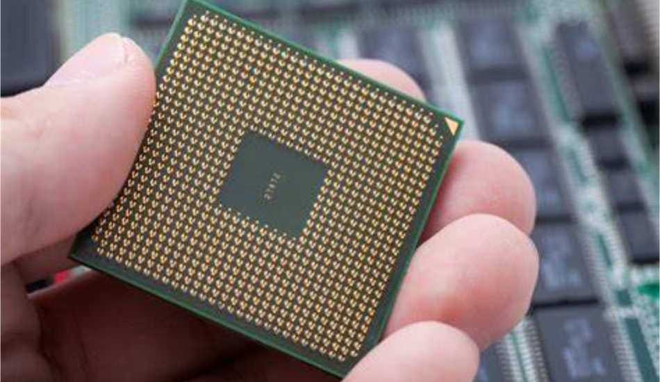
Improving Circuit Density with High-Density Interconnect Technology
Printed circuit boards (PCBs) are essential components in nearly all modern electronics. As devices continue getting smaller and more powerful, there is an increasing need to fit more circuitry into the same or even smaller PCB footprint. This is where high-density interconnect (HDI) PCB technology becomes critical.
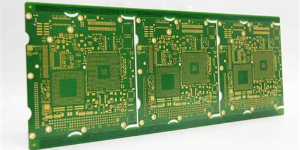
HDI PCBs provide higher component density, allowing more components and connections to be packed into a given area. This is achieved by reducing trace widths and distances between traces, as well as using thinner dielectric material between layers. HDI technology enables PCBs with finer features, more layers, microvias, and higher connection densities compared to standard PCBs.
Benefits of Using HDI PCBs
Here are some of the key benefits that HDI PCBs provide:
- Higher component density: More components and connections can be fit into a given PCB footprint area. This helps minimize the size of electronic devices.
- More routing channels: With thinner dielectric materials, HDI PCBs can have more routing layers in a given thickness. This allows for more signal traces to route connections between components.
- Finer features: HDI technology allows for finer line widths and spaces, smaller vias, and higher connection densities. Traces and spaces down to 15-20 microns are common.
- Improved performance: With shorter trace lengths, HDI PCBs can operate at higher frequencies while maintaining signal integrity. This improves speed and performance.
- Reduced EMI: Closer component spacing and dense power planes help contain electromagnetic interference (EMI). This improves reliability and compliance with emissions regulations.
- Lower costs: By fitting more components and connections into a smaller PCB, HDI technology effectively reduces assembly materials and costs.
HDI PCB Construction and Features
There are several key construction differences that distinguish HDI PCBs from standard PCBs:
Layer Stackup: HDI PCBs have specialized layer stackups optimized for routing density. A typical HDI stackup contains more layers overall, with most layers used for traces and ground/power planes:
- Signal layers: Thinner dielectric materials like polyimide allow more signal routing layers. There are typically 6-12 routing layers.
- Blind/buried vias: Vias connect between layers without going through the entire PCB. This allows more routing flexibility.
- Power and ground planes: Complete power and ground planes provide noise isolation andStable power delivery.
Trace/Space Width: HDI PCBs have finer trace widths and spaces between traces. While standard PCBs have minimum features around 4-5 mils (0.1 mm), HDI PCBs can achieve 2 mil (0.05 mm) traces and spaces.
Microvias: Microvias with diameters under 0.15mm help connect routing layers without requiring surface area. This provides vertical connectivity in tight spaces.
Laser Drilling: Microvias are typically drilled with laser systems to achieve the precision needed at these miniature sizes. Mechanical drilling is less capable of drilling small vias consistently.
Thin Dielectrics: Polyimide and other flexible dielectrics as thin as 25-50μm are used as insulators between layers. Thinner dielectrics allow closer trace spacing and more layers.
Fine Line Copper: Trace conductors use thin copper around 15-20μm rather than the typical 35μm copper foil. Finer features are patterned in the thinner copper.
Applications of HDI PCB Technology
With their higher densities and miniaturization capabilities, HDI PCBs are widely used in space-constrained and high performance products, including:
- Smart phones
- Tablets/laptops
- Wearable devices
- Internet of things (IoT) devices
- Medical electronics
- Automotive electronics
- Aerospace avionics
HDI PCBs are especially critical when there are requirements for small size, light weight, high speed, and reliability. The combination of more layers and high component density in HDI technology makes them well suited for complex, dense designs.
HDI PCB Design and Fabrication Considerations
While HDI PCBs provide major density and performance benefits, they also introduce some design and manufacturing challenges:
Design Complexity: HDI PCB layouts are more complex with detailed requirements for trace widths, spaces, microvias, and layer transitions. This can complicate routing and require advanced CAD tools.
Manufacturing Tolerances: The fine features in HDI PCBs have tighter tolerances. Fabricators require precise process control to produce HDI designs consistently.
Testing and Inspection: High-density components and micro features make it more difficult to fully test and inspect HDI PCBs. Specialized tools are required for reliability.
Thermal Management: Dense HDI boards can run into thermal issues without careful planning for component heat dissipation. This may require thermal vias, ground planes, and other cooling methods.
Cost: While HDI PCB assembly costs can be lower, fabrication of full HDI boards initially costs more than conventional PCBs. Designers must balance density with budgets.
Major HDI PCB Manufacturers
Many PCB manufacturers around the world have developed HDI technology and services. Some of the leading companies offering advanced HDI capabilities include:
- TTM Technologies
- Compeq
- Unimicron
- AT&S
- Ibiden
- Tripod Technology
- WUS Printed Circuit
- Zhen Ding Tech
To fabricate complex HDI PCB designs successfully, it is critical to carefully select a manufacturing partner with proven HDI experience, consistent processes, rigorous quality systems, and advanced production equipment.
The HDI PCB Fabrication Process Step-by-Step

Producing advanced HDI PCBs requires specialized fabrication techniques to achieve the tight tolerances and reliability required. Here is an overview of the manufacturing process steps:
1. Design and Layout
- The circuit requirements are developed into an HDI board layout using PCB CAD software.
- The design incorporates the fine trace widths, microvias, and layer transitions needed.
- Electrical, thermal, and mechanical modeling verifies the design’s performance.
- Gerber and drill files are generated to hand off to fabrication.
2. Laser Drilling
- A laser drilling system is used to produce the small microvias needed, typically under 150μm diameter.
- Laser drilling provides the precision and accuracy needed for HDI microvia formation.
- Different laser wavelengths, pulse widths, and drilling techniques are used based on the material.
- Registration accuracy is critical to drill the many thousands of holes in the right locations.
3. Metallization
- Electroless copper is used to first seed conductive material on the via walls.
- Electrodeposition then plates copper up the wall to the full via thickness required.
- The thin dielectric materials can make achieving a proper plated copper fill challenging.
- Filling agents may be used to assist with via plating throwing power and void reduction.
4. Layer Lamination
- Prepregs and dry film dielectrics are precisely laminated together under high heat and pressure.
- Precise pressure control prevents squeezing material into fine features or introducing warp.
- Some critical signals may require lamination of precisely aligned fine line cores.
5. Pattern Plating
- A photoresist is applied and imaged to form a plating mask for the traces and features.
- Fine line copper is then flash plated to build up the conductors to around 20-25μm.
- The plating process must completely fill openings and provide uniform thickness.
6. Etching
- Etching chemistry and the process are tuned to cleanly remove thin copper without undercutting traces.
- The conveyorized spray etching process requires precise temperature and chemistry monitoring.
- Cleaner etching improves fine space tolerances and minimizes open circuits.
7. Solder Mask & Legend
- Liquid photoimageable (LPI) solder mask accurately coats the PCB surface.
- Solder mask openings are aligned to exposed pads using laser direct imaging (LDI).
- Legend printing applies markings using inkjet printing registration cameras.
8. Final Finish
- Organic solderability preservative (OSP) provides a solderable surface while protecting copper traces.
- Nickel/gold plating can also be applied for some applications requiring it.
- Automated optical inspection (AOI) verifies all features are formed correctly before completion.
9. Electrical Testing
- Flying probe or bed-of-nails testers perform in-circuit testing of the boards for any connectivity defects.
- Continuity tests check for any opens or shorts. Boards must pass complete testing before shipment.
Throughout the entire fabrication process, high levels of automation, precision process control, and inspection are used to maintain the tight tolerances needed for HDI production.
Key Factors in HDI PCB Design and Material Selection
To successfully design an HDI PCB and select the right materials, there are several important considerations:
Signal Integrity: With higher speeds, signal integrity practices like impedance control, layer stack planning, and termination become critical. Simulations should validate performance.
Routing Density: More routing channels and microvia connections allow higher component densities. But too much density can also cause issues.
Signal Control: Tuning trace width and space controls impedance for matching. Minimize length differences between signals in groups.
Plane Layers: Full power and ground planes provide decoupling capacitance and noise shielding while also acting as a thermal sink.
Dielectric Materials: Properties like loss tangent and Z-axis CTE impact high-speed signal propagation. Stable, low-loss materials are preferred.
Thermal Management: Carefully plan out component heat dissipation methods like thermal vias, ground planes, and heatsink areas. model thermals.
Manufacturability: Account for manufacturability early when selecting layer count, thicknesses, and other stackup decisions that impact fabrication.
| HDI Design Parameter | Key Considerations |
|---|---|
| Board Thickness | Thinner dielectrics allow more layers in a given thickness. But too thin risks fragility. |
| Layer Count | More layers enable greater routing density. But each added layer increases cost. |
| Dielectric Materials | Materials with stable electrical and mechanical properties are preferred, e.g. polyimide. |
| Trace Width/Space | Match to fab capabilities. Finer features allow density but shrink tolerances. |
| Microvias | Essential for HDI layer transitions. Balancing size, number, and via tenting avoids reliability risks. |
| Layer Planes | Planes isolate signals while providing power delivery and thermal dissipation. |
By considering these factors early when architecting the board stackup and layout, HDI designs can achieve the right balance of density, performance, and reliability.
HDI PCB Design and Layout Best Practices
Here are some key PCB layout techniques and strategies to employ when designing complex HDI boards:
- Plan routing layers around signal groups: Keep related signals on common layers to simplify routing transitions and via connections.
- Leverage blind/buried vias: Use them to transition between signal layers without consuming external surface area.
- Build transfers across planes: Where signals change layers, traverse ground/power planes to provide shielding.
- Use parallel impedance paths: Match trace widths and spacing to desired single-ended impedance for controlled impedance routing.
- Tune routing for matched lengths: Minimize length differences between traces in each signal group.
- Watch component placement density: Ensure adequate spacing around heat generating components for cooling.
- Reduce surface mount land patterns: With fine ball grid arrays, land sizes can be shrunk significantly.
- Include test points: Provide adequate test access since troubleshooting HDI boards is difficult.
- Model the design: Perform signal and thermal modeling of the HDI board to validate performance before fabrication.
Proper HDI design practices will help avoid issues with signal performance, power delivery, thermal management, and manufacturing yield.
HDI PCB Challenges and Solutions
While HDI PCB technology provides major benefits, it also introduces some unique challenges. Here are some of the key issues along with mitigation strategies:
Routing Congestion: The sheer density of traces, vias, and components makes routing difficult. Solutions involve planning critical nets first, using all layers, and component rearrangement.
Signal Integrity: With high speeds over thin dielectrics, reflections and impedance discontinuities can cause major signal issues. Extensive SI modeling, controlled impedance routing, and termination are required.
Thermal Issues: High power components tightly packed will overheat without proper heat spreading and dissipation. Thermal vias, ground planes, airflow, and heatsinks help manage temperatures.
Manufacturing Defects: Thin materials and dense features increase fabrication defect risks. Stringent process controls, inspection, and quality systems minimize manufacturing issues.
Coplanarity: With many thin layers, warpage across the board can lead to non-coplanar surfaces and assembly problems. Warp-resistant core materials prevent this.
Test Access: Providing physical test access is difficult on dense boards. Strategies involve partitioning for divide-and-conquer testing and including debug/programming headers.
EMI Control: Noise coupling happens easily with minuscule trace separation. Careful stackup design, shielding, filtering, and enclosure design are required to control emissions.
With thorough design reviews, analysis, modeling, testing, and tightly controlled fabrication processes, potential HDI PCB issues can be identified and addressed early to ensure reliable performance.
Frequently Asked Questions
What are some key differences between HDI and standard PCBs?
HDI PCBs have smaller features and spacing, more routing layers, microvias, thinner dielectrics for increased density, and specialized fabrication processes to produce these dense designs reliably.
How small can trace widths and spaces be on HDI boards?
It is typical to achieve 2 mil lines and spaces. Some advanced HDI can reach 1 mil width and space dimensions. The limits depend on the manufacturer’s capabilities.
Why is laser drilling used to form microvias in HDI PCBs?
Laser drilling provides the precision and accuracy to reliably produce the large numbers of tiny microvias under 150μm diameter found in HDI boards.
What are the main dielectric materials used in HDI boards?
Polyimides are most common due to their stable electrical properties. Others include bismaleimide triazine (BT), liquid crystal polymer (LCP), and fluoropolymers like PTFE.
What design factors are most important when working with HDI PCBs?
Account for signal integrity, impedance control, thermal management, manufacturability, layer planning, and modeling accuracy early when architecting HDI designs.
How are HDI PCBs tested given their density?
Flying probe testing, boundary scan, and partitioning the design to simplify testing access are key strategies. Build in debug/programming headers for access.
Conclusion
As electronic devices continue getting more compact and complex, HDI PCB technology enables the level of miniaturization and component density needed. By reducing feature sizes and dielectric thicknesses while adding more layers, HDI provides a powerful platform for advanced electronics.
However, realizing the full benefits of HDI requires attention to detail in design, material selection, modeling, manufacturability, and quality control. When implemented successfully, HDI PCBs deliver higher performance and reliability in a smaller footprint to meet growing market demands. The techniques outlined here capture current best practices for harnessing HDI technology effectively.


Leave a Reply