Introduction
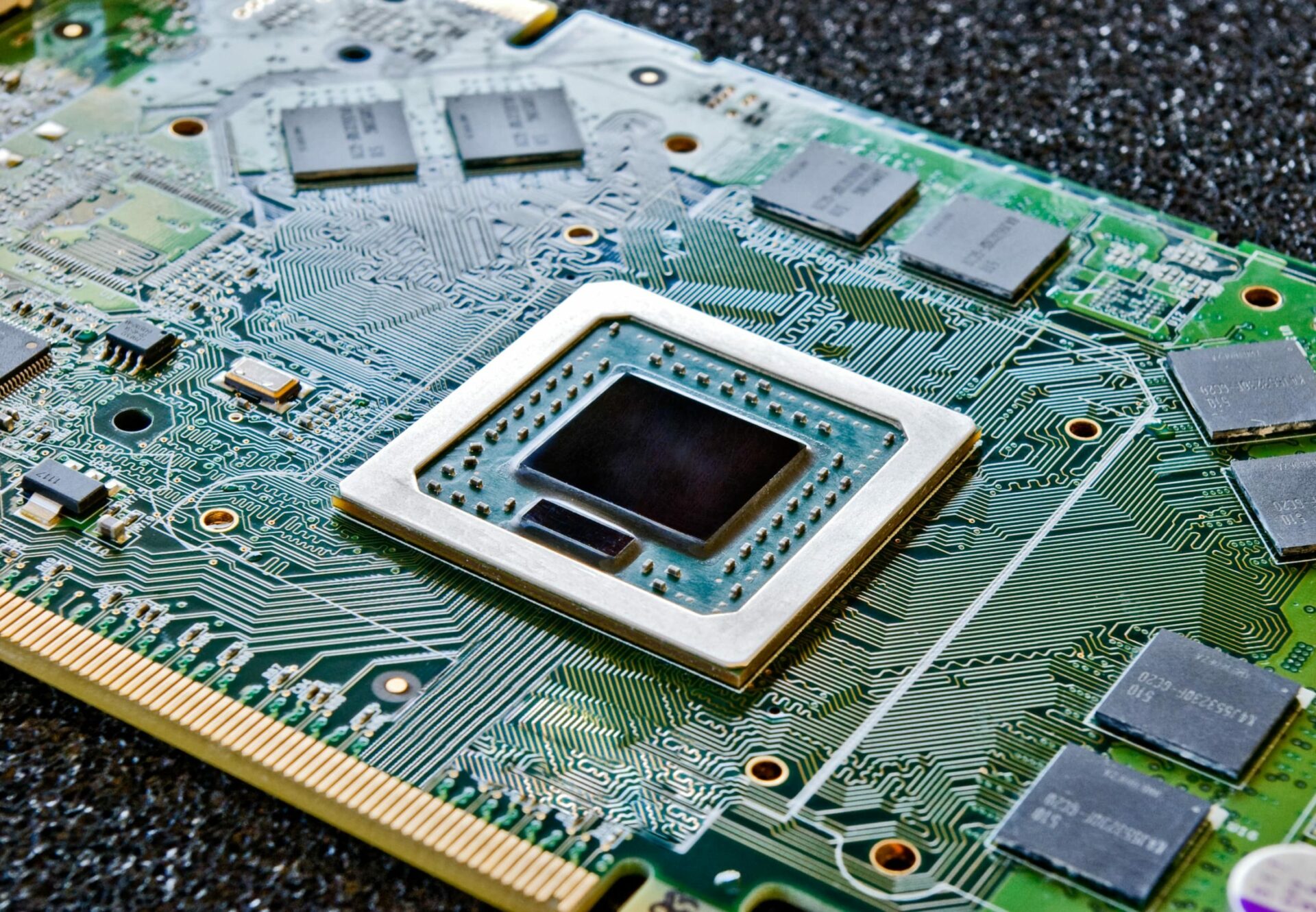
HDI (high-density interconnect) PCBs (printed circuit boards) are an advanced form of PCB that allow components to be packed more densely on the board. HDI technology enables thinner traces, smaller vias, and more layers, which allows for greater component density and more complex circuit designs.
In this guide, we will cover the key aspects of HDI PCB design and manufacturing. Topics will include:
- The benefits of using HDI PCBs
- HDI design rules and constraints
- Stackup construction and layer planning
- HDI routing techniques
- HDI materials and fabrication processes
- HDI testing and inspection
Understanding these topics will help you design compact and reliable HDI boards to meet the needs of space-constrained and complex electronic devices.
Benefits of HDI PCBs
HDI PCBs provide several advantages over traditional PCBs:
Smaller Components and Traces
HDI technology allows the fabrication of extremely fine lines and spaces. Traces and spaces down to 3/3 mils (0.15mm) are possible with HDI processes. This enables smaller pad sizes and routability of finer pitch components.
Higher Component Density
The finer features of HDI PCBs allow components to be packed more densely. Component density of over 2000 components per square inch is possible. This helps minimize the PCB footprint for space-constrained devices.
More Routing Layers
HDI PCBs utilize more routing layers. 6-12 layers are common for HDI boards. This provides more space for traces and allows for shorter, optimized routing paths.
Advanced Electrical Performance
With tightly controlled impedances, matched lengths, and low crosstalk, HDI PCBs enable advanced high-speed design up to multi-GHz frequencies. This makes them suitable for RF, microwave, and other high-frequency applications.
Lower Weight and Thickness
HDI PCBs can be fabricated thinner than standard boards. As component density increases, overall board size and weight is reduced. This saves space and weight in portable and compact devices.
Improved Reliability
The materials and fabrication processes used for HDI boards result in quality construction with strong adhesion between layers. This improves mechanical and thermal performance.
HDI Design Rules and Constraints

To achieve a reliable, manufacturable HDI PCB design, certain design rules and constraints must be followed:
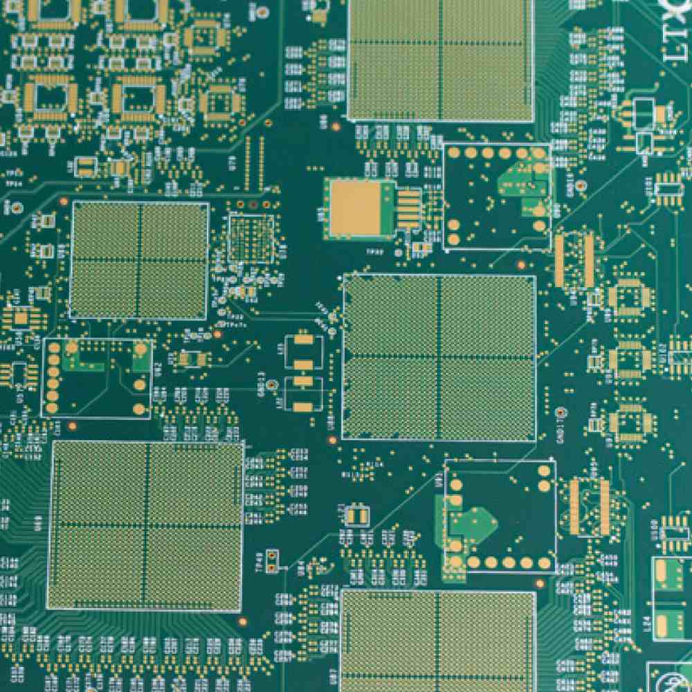
Trace/Space Width and Clearance
The minimum trace/space is typically 4/4 mils down to 3/3 mils. For high volume boards, 5/5 mils is more readily achievable. The minimum clearance between adjacent traces is normally 3 mils.
Via Sizes and Pads
Microvias with 4-8 mil holes and 6-12 mil pads are common. Stacking microvias requires laser drilling for reliable connections between layers.
Component and Pad Sizes
Chips and passive components down to 0201 inch size can be accommodated. Pads and component lead pitches down to 4 mils are feasible.
Aspect Ratios
High aspect ratio laser drilling (>10:1) is used to achieve the necessary fine via holes while maintaining mechanical drill integrity. This places constraints on the via placement.
Annular Rings
A 1 mil annular ring (pad-to-hole clearance) is typical for microvias. This helps avoid opens and reliability issues.
Slots and Cutouts
Slots narrower than 5 mils can impact structural strength and should be avoided. Small cutouts can hinder drilling quality, so larger keepouts are advised.
By following the design guidelines, you can create a manufacturable HDI board that meets your density and performance requirements. Work closely with your PCB manufacturer to ensure your design adheres to their capabilities.
HDI Stackup Construction and Layer Planning
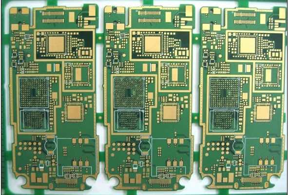
The stackup, or layer structure, of an HDI PCB requires careful planning. Here are some key stackup design considerations for HDI boards:
Layer Thickness and Count
HDI boards have more layers than standard PCBs. High layer counts are needed to route dense designs. Typical constructions are 6 to 12 layers. Thinner dielectric materials (3-5 mils) allow for more layers in a given thickness.
Microvia Layers
At least one microvia layer is required to connect surface traces to internal layers. More microvia layers provide additional vertical routing capability. Blind and buried vias require additional steps, so minimizing these via types helps reduce cost.
Power and Ground Layers
Multiple power and ground plane layers help provide clean power distribution at high frequencies. A simple four-layer stackup may use layers 2 and 3 for power/ground. In higher layer count boards, several mid-layers can be assigned to power/ground functions.
Signal Layers
Signal layers in between power and ground planes should be used for critical high-speed routing. Match lengths by routing differential pairs on the same layer. Adjacent signal layers should be avoided to prevent coupling.
Component Layer Types
SMD components can be placed on one or both sides. Double-sided placement increases density. BGAs with microvia connections to inner layers are common. Some components may require cavities or cutouts in inner layers.
Layer Sequence
The layer order should generally go power-signal-ground-signal-power to provide shielding and isolation between signals. Certain high-speed nets may warrant being adjacent to reference planes.
Careful stackup design provides the layer types and sequence needed for optimized routing, power integrity, and signal performance.
Example 6-Layer HDI Stackup
| Layer | Function |
|---|---|
| 1 | Signal |
| 2 | Ground |
| 3 | Power |
| 4 | Signal |
| 5 | Ground |
| 6 | Signal |
HDI Routing Techniques
With multiple routing layers and components tightly packed, HDI PCB layout requires special techniques to successfully route all connections:
Grids and Component Placement
Use small grid settings matching your minimum spacing/clearance rules. Place components optimally, keeping high-speed nets short and grouping by signals. Watch for “dead zones” with limited access.
Build Planes First
Prioritize power and ground planes to ensure a solid reference structure before routing critical signals. Use area fills rather than polygons. Check plane isolation.
One Net Per Layer
Route one differential pair or critical signal net per layer as much as possible. Minimize vias and crossovers to reduce interference.
Microvias and Stacking
Use microvias to transition between outer and inner layer signals. Laser-drilled stacked microvias provide connections between non-adjacent layers.
Length Matching
Match electrical lengths by routing differential pair traces together. Serpentine and meander paths help tune lengths.
Fanouts and Escape Routing
Plan fanouts and breakouts carefully on dense boards. Use angled traces, microvias, and zero-ohm resistors as needed for creative escape routing.
Minimize Crossovers
Reduce crosstalk by minimizing trace crossovers, especially on outer layers where microvia transitions induce discontinuities.
Reduce Jogging
Limit the number of trace jogs which perturb signals, cause reflections, and hinder impedance control. When needed, use 45-degree angles.
Manual Routing
Use manual routing for critical nets to achieve precise control. Autorouters may not meet impedance, length, or crosstalk requirements.
With good component placement and routing practices tailored to HDI, you can successfully interconnect even the densest designs. Verify routing meets specifications with electromagnetic simulation.
HDI Materials and Fabrication Processes
To manufacture reliable HDI boards capable of extremely fine features, specialized materials and fabrication techniques are required.
Dielectric Materials
The dielectric layers are fabricated from low-loss materials such as polyimide and liquid crystal polymer (LCP). These provide tight impedance control and consistent performance up to microwave frequencies.
Conductive Layers
Electroplated copper foils as thin as 1/2 oz (18 um) are used along with laser-drilled microvias to produce fine traces and spaces. Thin cores reduce layer thickness. Direct metallization processes can eliminate copper foil.
Sequential Lamination
Dielectrics and copper foils are laminated together one layer at a time. This allows materials tailored for performance, thickness, and flatness to be used for each layer.
Laser Drilling
A CO2 or UV laser is used to ablate microvias through multiple dielectric layers. Tight hole size tolerances and high aspect ratios (>10:1) are possible. Stacked microvias are cleanly formed.
Plating and Metallization
Conformal copper plating of microvias and fine features is critical to achieve reliable interconnects. Both electroless and electrolytic copper processes are used along with direct plating methods.
Final Surfaces
Organic solderability preservative (OSP) or other surface finishes are applied to provide solderability while allowing probing for test. Gold plating is sometimes used for wire bonding.
Automated Optical Inspection (AOI)
Sensitive AOI tools detect defects in traces, vias, spacing, and other features. Tight process controls and inspection ensure reliability.
By combining specialized materials with precise fabrication techniques, HDI’s demanding design rules can be met.
HDI Testing and Inspection
Verifying the fabrication quality and electrical performance of HDI boards requires advanced testing and inspection:
Microsectioning
Cross-sectioning and microscopy validates proper layer alignment, individual layer thickness, plating quality, and drill integrity.
Automated Optical Inspection (AOI)
AOI tools with high magnification and image processing algorithms are used to inspect trace widths, spacing, openings, and other small features for defects.
Electrical Testing
Flying probe or grid testing verifies shorts, opens, impedance, propagation delay, and other electrical parameters. Loaded board testing checks performance under operational conditions.
X-Ray Inspection
X-ray imaging allows inspection of buried features including microvia interconnects and plating quality. It is used to complement optical AOI for full defect coverage.
Surface Imaging
Scanning electron microscopy, laser profilometry, and other techniques provide nanometer-scale imaging of traces and drill quality. Surface morphology and roughness are evaluated.
Thermal Stress Testing
Thermal cycling, HAST, and/or solder reflow simulation tests verify structural and electrical integrity under temperature extremes and moisture exposure.
Along with testing the bare PCB, inspection of populated boards including X-ray and automated optical inspection of solder joints ensures quality assembly.
With the appropriate battery of tests targeted to HDI’s fine features, both manufacturing defects and potential field reliability risks can be detected prior to product release.
Frequently Asked Questions
Here are answers to some common questions about HDI PCB design:
What are the main advantages of HDI PCBs?
HDI PCBs allow higher component density, smaller features, improved high speed performance, lower weight/thickness, and greater routability compared to standard PCBs. This makes them ideal for compact, complex devices.
How small can traces and spaces be on HDI boards?
Traces and spaces down to 3 mils are possible, but 5 mils is more common for volume production. Microvias are typically 4-8 mils in diameter.
What are typical HDI layer counts?
Most HDI designs utilize 6-12 conductive layers. High layer counts provide routing capacity for dense, complex circuits. Thinner dielectrics allow more layers in a given board thickness.
What materials are used in HDI PCB fabrication?
Specialized low-loss, tightly controlled dielectrics such as polyimide are used. Very thin copper foils (~1/2 oz) enable fine features. Direct plating processes are also used.
How does an HDI PCB get moisture protection?
HDI boards often utilize laminated metal cores on the outer layers to provide shielding, some structural rigidity, and hermeticity against moisture and other contaminants.
Does HDI technology require special design expertise?
Yes, HDI layout is a specialized skill. Work closely with an experienced PCB designer familiar with HDI constraints. Partnering with a high-tech PCB fabricator is also advisable.
Conclusion
HDI PCB technology enables increased component density, high-speed performance, miniaturization, and routability of complex circuits. Realizing these benefits requires careful design according to HDI constraints, precision fabrication with special materials and processes, and robust testing and inspection. With the right expertise and fabrication partner, the capabilities of HDI can help you meet the needs of your cutting-edge electronic product designs.


Leave a Reply