Introduction to Hdi Pcb Boards
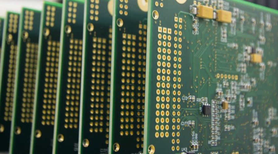
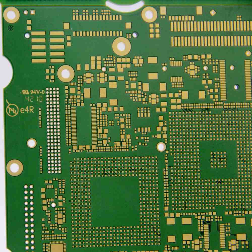
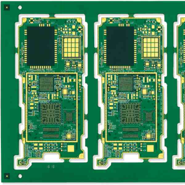
HDI (High Density Interconnect) PCBs (Printed Circuit Boards) are a specialized type of PCB featuring finer lines and spaces, smaller vias, and higher connection pad densities compared to conventional PCBs. HDI allows for denser routing, more compact layouts, and thinner circuit boards ideal for complex, compact electronics.
Some key characteristics of HDI PCBs:
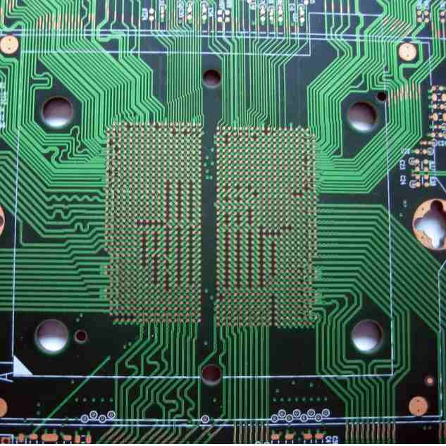
- Much finer trace widths and spaces – down to 3/3 mil (0.15mm) spacing
- Microvias with diameters as small as 0.15mm vs 0.30mm for conventional PCBs
- More routing layers – typically 6-12 vs 4-8 for conventional PCBs
- Higher pad densities facilitating high I/O counts
- Overall thinner boards due to thinner dielectric layers
- Improved signal integrity from closely spaced traces
HDI techniques enable miniaturization and integration for many advanced electronics. HDI PCBs are essential for products like smartphones, wearables, IoT devices, medical devices, and more.
Hdi Pcb Technology Overview
There are a few key technologies that distinguish HDI PCB fabrication and allow for the finer features and densities.
Laser Drilling
The microvias in HDI boards require laser drilling technology. Mechanical drilling cannot reliably produce microvias smaller than 0.15mm in diameter. Laser drilling uses a CO2 laser to ablate the dielectric layer and create these fine microvias. This allows for denser via patterns.
Thin Dielectrics
The dielectric material separating copper layers is much thinner in HDI boards. Typical dielectrics are 25-50 μm thick compared to 100 μm in conventional PCBs. This allows for more routing layers in a given thickness.
Finer Routing Traces
HDI PCBs achieve trace and space widths down to 3/3 mil spacing between traces. This is done through advanced photolithographic processes and materials. Finer traces enable dense routing channels.
Sequential Lamination
Each dielectric layer is laminated individually in HDI boards rather than all at once. This helps reduce stresses and improve reliability for the thin dielectrics.
PADS Design
HDI layouts require specialized design rules and CAD tools to implement the trace widths, spaces, and pad designs. PADS is a common PCB layout tool optimized for HDI.
Any-Layer Via Techniques
Any-layer microvias allow connections between any two layers rather than just adjacent layers. This improves routing flexibility.
Benefits of Using Hdi Pcb Boards
There are many benefits to selecting an HDI PCB for complex, miniaturized PCB designs:
- Higher component density – The finer features allow components to be placed closer together. This reduces the overall footprint of the populated board.
- Miniaturization – HDI allows for smaller and thinner overall PCB solutions due to the tighter spacing, higher layer count, and thinner dielectric layers.
- Improved performance – The shorter traces and vias reduce parasitic inductance and capacitance for better high-speed performance. Signal integrity also improves.
- Higher I/O counts – The dense microvias and traces support more signals routing to BGA, CSP, and other high pin count packages.
- More routing channels – Additional layers and dense traces create more routing channels for complex layouts. This can reduce or eliminate layer transitions.
- Lighter weight – The thinner profile reduces weight which is ideal for portable electronics.
- Improved reliability – Laser drilled microvias avoid issues associated with mechanical drilling like via cracks andresin smear.
Hdi Pcb Design and Layout Considerations
Designing and laying out an HDI PCB requires special design rules, constraints, and modeling. Here are some key considerations:
- Follow stringent design rules for trace width/space, annular rings, and anti-pad sizes. This is essential for manufacturability and preventing shorts.
- Model traces as transmission lines, not as ideal conductors. Controlled impedance is critical for high speed signals.
- Employ constraints for length matching, phase matching, and delay matching for differential pairs and high speed signals. This improves signal integrity.
- Use thermal modeling and analysis early in the design process. HDI boards can run hotter due to high densities.
- Determine layer stackup and sequence – 6 to 12 layers are typical including multiple ground and power planes. Include direct buried and blind/embedded vias as needed.
- Utilize EDA tools with native HDI support – Allegro, Xpedition, PADS, Altium etc. This checks design rules and modeling.
- Collaborate with your PCB fabricator early. They can offer stackup recommendations, DFM analysis, material selection, and modeling assistance.
- Plan for thorough testing and inspection. HDI fabrication tolerances are tight so testing for potential shorts, opens, and EMI is critical.
Hdi Pcb Design Software Tools
Many EDA (electronic design automation) software platforms now include specialized functionality to support HDI PCB design. Here are some of the most popular tools:
| Software | Key Features |
|---|---|
| Allegro PCB Editor | – Constraint manager <br>- RF design and analysis <br>- Manufacturing checks <br>- Stackup planning <br>- High speed modeling |
| Mentor Xpedition | – Rules and DFM checks <br>- Routing with auto-avoidance <br>- Library for HDI components <br>- Multi-channel length tuning <br>- Impedance and signal integrity |
| Cadence Allegro/OrCAD | – Manufacturing capabilities <br>- Constraint management <br>- RF design capabilities <br>- Interfaces with signal/power integrity tools |
| Altium Designer | – Native HDI design rules <br>- Length tuning <br>- Automatic backdrilling <br>- Modeling integrated into engine |
| PADS | – Dedicated HDI design flow <br>- Teardrop voiding <br>- Rules checking <br>- Embedded die support |
These tools help automate many aspects of HDI design from planning layer stackups through final DFM checks. Their HDI-specific capabilities help manage the tighter constraints while optimizing routing.
Hdi Pcb Fabrication and Assembly Process
Fabricating HDI PCBs requires advanced manufacturing techniques and precision equipment beyond typical PCB production:
- Laser direct imaging (LDI) pattern generators define the finer traces. Higher accuracy over traditional photomasks.
- Laser drills are used for creating the microvias in the dielectrics down to 0.10mm diameter or less.
- Thin core and prepreg dielectric materials keep layer thicknesses under 50μm.
- Buildup dielectric deposition done by qualified technicians for quality control. Tighter process control.
- Sequential lamination interleaves bare core, dielectric, and foil rather than all at once. Achieves better thin core adhesion.
- Microvia filling and capping may be done to protect small vias and prevent overplating.
- Plating equipment must achieve uniform copper distribution across tightly spaced traces.
- Etching processes require tight tolerances to prevent over-etching.
- Automated optical inspection (AOI) and testing is implemented given the high defect rates possible. Confirms design rule compliance.
- Impedance testing, microsectioning, and microvii inspection qualification performed.
- Precise lamination, drilling, and routing required for any embedded passive components.
The assembly process also requires advanced techniques:
- Tight component pitch requires specialized pick and place equipment. High accuracy and small nozzle.
- Underfill, corner bonding, and bottom termination may be used for reliability.
- X-Ray inspection can find hidden defects and confirm proper assembly.
- Leaded reflow or other assembly may be needed depending on part densities.
Hdi Pcb Design and Fabrication Cost Considerations
HDI PCBs carry higher costs compared to conventional PCBs due to their increased complexity. Here are some factors that contribute to cost:
- Design – More engineering time required for HDI design constraints and modeling. Advanced EDA software also carries higher license costs.
- Prototyping – More iterations may be needed to refine HDI stackup, design rules, and manufacturability.
- Fabrication – Tighter tolerances require advanced PCB equipment. More manual operations. Lower yields. More inspection and qualification steps.
- Materials – Base materials such as laminates are more expensive. Additional finishing steps like microvia filling also add cost.
- Qualification – Extensive testing throughout fabrication required for process control and DFM verification.
- Assembly – Precision placement, inspection, and secondary operations add cost. Lower initial yields.
According to one estimate, HDI PCB fabrication costs can be 2 to 4 times higher than standard multilayer PCBs. However, the long term savings from miniaturization, improved performance, and higher reliability usually outweigh the higher production costs.
Common Problems With Hdi Pcbs
While offering many benefits, HDI PCB technology also introduces some potential failure modes and reliability risks:
- Moisture absorption – The thin dielectric layers absorb more moisture which can cause delamination and barrel cracking when assembled.
- Via cracks – Microvias are prone to fracturing which can cause opens. Typically induced by residual stresses.
- Resin recession – Dielectric resin around microvias can recede leading to reduced spacing and potential shorts.
- Underplating – Incomplete plating inside microvias can create weak spots leading to early field failures.
- Lower peel strength – Delamination issues are more likely with the thinner dielectric buildup materials used.
- Tombstoning – More prone to tombstoning of small passives during assembly due to thinner profile.
- Thermal stresses – Higher local densities can create thermal gradients leading to warping or cracking under temperature cycling.
Proper design rules, modeling, process control, inspection, and qualification is key to minimizing these potential issues in HDI boards.
Frequently Asked Questions
What are some typical applications for HDI PCBs?
Some of the most common applications are consumer electronics like smartphones, tablets, wearables, drones, and Internet of Things (IoT) devices. They are also used in high-speed computing and network systems, medical devices, aerospace and defense electronics, instrumentation, and automotive electronics.
What layer count is typical for HDI designs?
HDI designs typically range from 6 to 12 routing layers depending on complexity, I/O requirements, and other factors. Some may go up to 20 layers for very dense designs. The layer count needs to be optimized based on a tradeoff between routing complexity, board thickness, and fabrication costs.
How are microvias formed in HDI PCBs?
Laser ablation is used to selectively remove the dielectric material and create microvias smaller than 6 mils diameter in HDI boards. CO2 lasers operating at wavelengths around 10 μm are commonly used for drilling organic PCB materials.
Can components be embedded in HDI PCBs?
Yes, HDI manufacturing allows for integrated embedded components like capacitors, resistors, and even ICs or LEDs. This provides further miniaturization and improved electrical performance by eliminating discrete SMT components. The components are placed into cavities in the bare core layers before lamination.
Does HDI allow for higher operating frequencies?
The tightly spaced traces, thin dielectrics, and dense vias in HDI PCBs significantly reduce parasitic inductance and capacitance. This allows them to support higher signal frequencies well above 5GHz compared to traditional PCBs limited to ~1-2GHz.
Conclusion
HDI PCB technology enables denser, higher performance, and more reliable PCB solutions critical for the miniaturization of modern electronic devices through finer features sizes, laser microvias, additional routing layers, and advanced design and manufacturing techniques. As electronics continue trending toward ever greater compactness and complexity, HDI will become increasingly prevalent across the industry. Companies must consider both the benefits and challenges of incorporating HDI into their products. With careful HDI design and qualification, the rewards are well worth the investment for many advanced PCB applications.


Leave a Reply