Introduction
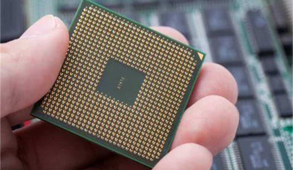
High density interconnect (HDI) PCBs have become increasingly common in consumer electronics and other electronic devices where space is at a premium. HDI allows for denser routing between components, enabling smaller and more compact PCB designs.
One configuration of HDI PCBs is known as 2+N+2, referring to the number of conductive layers. This article will examine what defines a 2+N+2 HDI PCB and discuss the benefits and challenges of designing and manufacturing moderate complexity HDI boards in this configuration.
What is a 2+N+2 HDI PCB?
A 2+N+2 HDI PCB contains 4 outer layers and N number of inner layers for routing signals and power. The outer layers are configured as follows:
- Layer 1 (Top Layer): Primarily used for SMT component placement and routing
- Layer 2 (Power Plane Layer 1)
- Layer N+2 (Power Plane Layer 2)
- Layer N+3 (Bottom Layer): Primarily used for routing and PTH component placement
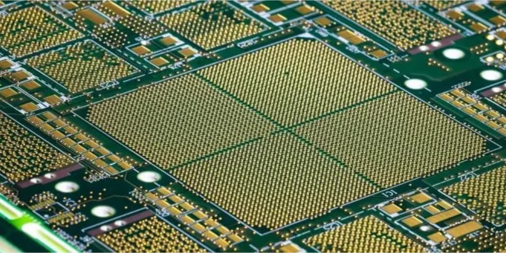
The inner layers from Layer 3 to Layer N are all signal layers used for routing traces between components. A typical layer stackup is shown below:
Table 1: 2+N+2 HDI Layer Stackup
The major benefits of the 2+N+2 configuration are:
- Good signal isolation since signals are sandwiched between power and ground planes
- Moderate layer count keeps costs lower compared to higher layer count HDI
- Balance between signal routing capacity and manufacturability
Moderate Complexity 2+N+2 HDI
Moderately complex 2+N+2 HDI PCBs strike a balance of leveraging HDI technology while minimizing risk and cost. Here are some typical attributes of moderate complexity 2+N+2 HDI boards:
- Fine Lines/Spaces: 12/12 mil line/space is common, with some use of 8/8 mil lines in critical areas
- Via Sizes: 8 to 10mil microvias, 10 to 12mil buried vias
- Routing Density: Moderate routing densities, usually between 20-60% on inner layers
- Pad/Anti-pad Designs: Normal functionality pad/anti-pad sizes used, no areas of ultra-fine pitch I/O
- Layer Count: Typically 4-8 layers
- Materials/Stackup: Standard FR-4 dielectric materials, conventional constructions
By combining fine features with a modest layer count and conventional materials, moderate 2+N+2 HDI provides a cost-effective balance for many applications. The relatively large microvias and lack of extremely dense routing or ultra-fine pads/spaces also allows these boards to be manufactured with good yields.
Benefits of Moderate Complexity 2+N+2 HDI
There are several advantages to using a moderate complexity 2+N+2 HDI approach:
Space Savings
- Finer routing allows components to be placed closer together
- Microvias take up less space compared to through hole vias
- Overall footprint of the PCB can be reduced
Routing Capacity
- More routing channels with additional layers
- Finer traces allow more routes to be packed into the same area
Signal Integrity
- Shorter trace lengths due to space savings
- Microvias have less parasitic effects than through holes
- Power plane sandwich provides noise isolation
Cost
- Moderate layer counts control costs
- Conventional materials are less expensive
- Good manufacturability minimizes scrap losses
The more modest capabilities help contain costs while still providing substantial gains in performance, space utilization, and signal quality compared to a conventional PCB.
Challenges with Moderate Complexity 2+N+2 HDI
While the compromises made help moderate complexity 2+N+2 HDI deliver value, some challenges can arise:
Routing Congestion
The finer features help, but routing congestion can still occur in complex designs with high pin counts. Careful floorplanning is essential.
Via Reliability
Microvias require precise drilling and plating to ensure reliability. Some marginal yield loss may occur.
Signal Integrity Testing
With faster edge rates, SI analysis and testing are recommended to validate performance.
Thermal Management
Higher component densities increase thermal challenges. Thermal vias, copper fills, and other cooling methods help.
Fabrication Expertise
Not all fabricators have 2+N+2 HDI process capability. Care should be taken in selecting a qualified PCB manufacturer.
While these factors require attention, they can be mitigated with an experienced design team.
Applications for Moderate Complexity 2+N+2 HDI

Here are some examples of products that can benefit from a moderate complexity 2+N+2 HDI approach:
- Wireless Communications Equipment
- Consumer Electronics
- Automotive Electronics
- Industrial Controls
- Medical Electronics
- Test and Measurement Equipment
The demands for miniaturization, performance, reliability, and cost control make moderate 2+N+2 HDI a good fit for these applications. The technology provides a robust PCB solution without the complexity risks and costs of more advanced HDI.
Design Guidelines
Here are some key design guidelines to follow for a successful moderate complexity 2+N+2 HDI board:
Floorplanning
Carefully floorplan component placement and routing paths to minimize length and congestion. Plan power distribution early.
Routing Rules
Use conservative trace width/spacing rules. Minimize length differences between data pairs. Build in impedance matching where needed.
Stackup
Work with your PCB manufacturer to define an appropriate layer stackup based on signal isolation needs and plane current.
Via Transitions
Limit via stubs. Plan via barrel size and anti-pad dimensions carefully for goodSignal integrity.
Manufacturing Analysis
Have your fabricator review the design. Make adjustments based on their capabilities and suggestions.
Following these guidelines will help avoid issues and ensure a successful project.
Summary
Moderate complexity 2+N+2 HDI provides an excellent combination of density, performance, cost, and manufacturability for many advanced PCB designs. By leveraging fine features while minimizing layer counts and advanced technologies, it delivers substantial benefits without excessive risks. Careful floorplanning, routing, and manufacturer collaboration when designing in this technology will lead to successful PCB implementation.
Frequently Asked Questions
What are some key differences when migrating from conventional PCB to moderate complexity 2+N+2 HDI?
Some of the major differences include:
- Using microvias instead of through hole vias
- Routing traces on higher layer count
- Tighter routing geometries required
- Minimizing via stubs
- Potentially new design rules on spacing/width
- Attention to impedance on critical signals
- Fabricators with specific HDI qualifications
It represents an increase in design complexity that should be evaluated thoroughly before migrating.
What layer count range is typical for moderate complexity 2+N+2 HDI?
Usually moderate 2+N+2 HDI designs have 4-8 conductive layers. This provides a good compromise between routing capacity and controlling fabrication costs. High pin count or very dense designs may need higher layer counts, but numbers above 8 tend to drive increased risk and cost.
How are microvias used on a 2+N+2 HDI PCB?
Microvias are small vias (8-12mil diameter) that connect between layers. They can connect surface layers to the first adjacent plane layer or stitch between internal layers. Laser drilling and precise plating/filling processes are used to reliably produce them during fabrication. Using microvias instead of through holes is what allows the increased routing density.
What design software is typically used for moderate complexity 2+N+2 HDI?
Most PCB designers use standard tools like Cadence Allegro, Mentor Xpedition, or Altium Designer. The tools incorporate HDI design rules to assist with trace widths, clearances, and via designs. Some additional analysis or modeling software may be used for signal or power integrity simulation on critical HDI boards.
What are some key fabrication process steps to make 2+N+2 HDI PCBs?
Critical processes include laser drilling of microvias, plasma treatment of dielectric surfaces, and precise copper plating processes. Layer alignment is also very important, using advanced lamination and buildup processes. Testing procedures like microsectioning and automated optical inspection help ensure reliability. HDI processes require significant expertise and capital investment from the PCB fabricator.


Leave a Reply