Introduction
Printed circuit boards (PCBs) are fundamental components of modern electronics, providing the physical platform upon which components are mounted and connected. As electronic devices continue to shrink in size while increasing in capability, the density of components and interconnects on PCBs has steadily increased. This has driven the development of high-density interconnect (HDI) PCB technologies to accommodate the high input/output (I/O) density requirements of advanced electronics.
One rapidly emerging HDI technology is 2N2 PCBs. 2N2 refers to a construction utilizing two routing layers on either side of an HDI core, for a total of two signal layers on the top and bottom surfaces. This article provides an overview of 2N2 HDI PCB technology, including its architecture, fabrication, benefits, and applications driving its increasing use.
HDI PCB Architecture
HDI PCBs utilize thinner dielectric buildup materials layered onto a thick, rigid core layer. This allows higher interconnect density compared to conventional PCBs, as conductors can be spaced more closely together. Vias also utilize microvias with smaller diameters, allowing denser via distribution.
The 2N2 architecture consists of a central HDI core layer, which is a thin laminate dielectric. On either side of this core are two layers of fine line/spacing interconnects. There are no buried via layers within the 2N2 construction. Connections between the top and bottom sides are made through microvias drilled into the core layer. This is depicted in the diagram below:
Figure 1: 2N2 HDI PCB architecture showing central core with routing layers
Compared to other HDI arrangements such as 3N3 (three routing layers on either side of the core) or 4N4, the 2N2 design allows similar interconnect density with a simpler overall construction. The thinner profile is also beneficial for space-constrained and high-speed designs.
Fabrication and Materials
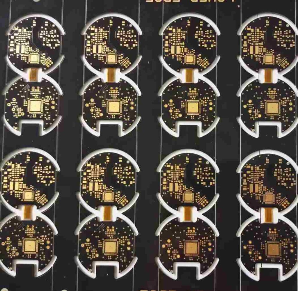
There are several key fabrication processes and material choices that enable reliable 2N2 HDI boards:
- Thin core dielectric – The HDI core layer is typically made from advanced dielectric materials such as polyimide or liquid crystal polymer (LCP). These maintain stability and performance at core thicknesses down to 25-50μm.
- Microvia drilling – Small microvias with diameters down to 50μm are laser drilled through the core layer to allow connections between the top and bottom routing layers. The via walls are plated to form the electrical connections.
- Thin dielectric buildup – Additional layers of thin dielectrics are added to either side of the core through lamination or deposition processes. These layers are typically 12-25μm in thickness.
- Fine line patterning – The exterior routing layers are patterned using advanced photolithography techniques to achieve fine lines and spaces less than 20μm. This allows high interconnect density.
- Plating and etching – The conductive traces and vias are formed by plating followed by etching to define the circuit pattern. Solder mask and surface finishes complete the board fabrication.
Benefits of 2N2 HDI
The 2N2 architecture provides several benefits that make it attractive for advanced PCB designs:
- Simplified layout – The lack of buried vias simplifies routing by avoiding connectivity obstacles within the layers. This can make layout faster and more efficient.
- High interconnect density – The thin dielectric layers and fine line/spacing traces allow a high concentration of interconnects. This enables complex, high-pin count component mounting.
- Good high-speed performance – Properly designed 2N2 boards can achieve excellent signal integrity up to 25+ Gbps data rates. The thin, symmetrical stackup is beneficial for controlled impedance interfaces.
- Lower costs – 2N2 boards reduce costs compared to equivalent 4N4 designs by requiring fewer lamination cycles and process steps during fabrication. This makes HDI technology more accessible.
- Thinner profiles – The simplified 2N2 structure results in a thinner overall board thickness. This helps reduce the z-axis footprint in space-constrained electronics packaging.
Applications Driving 2N2 Adoption
The combination of simplicity, performance, and cost-effectiveness is driving increased use of 2N2 HDI technology across a range of advanced electronics applications:
Consumer Electronics
- Smartphones
- Tablets/laptops
- Wearable devices
- Internet of Things (IoT) products
For consumer devices, 2N2 HDI allows integration of high I/O density components like processors, memory, and wireless chips in thinner and smaller packages. The boards are well suited for advanced packaging techniques like package-on-package (PoP).
Automotive Electronics
- Engine control units (ECUs)
- Infotainment systems
- Advanced driver assistance systems (ADAS)
- Electric vehicle (EV) power systems
HDI PCBs enable the increasing electronics functionality demanded by modern vehicles. 2N2 provides a simplified approach to achieve the interconnect density required in high-reliability automotive applications.
High-Speed Communications
- Networking/switching equipment
- Optical transceivers
- 5G wireless infrastructure
The excellent signal integrity of properly designed 2N2 boards makes this technology suitable for 25+ Gbps serial links using interfaces like PCIe, Ethernet, and more.
Aerospace/Defense
- Avionics equipment
- Vetronics (vehicle electronics)
- Radar and electronic warfare systems
Ruggedized 2N2 boards meet the high density and reliability demands of electronics operating in harsh military/aerospace environments. LCP-based cores provide thermal stability and resistance to extreme conditions.
Conclusion
2N2 HDI PCB technology enables increased interconnect density in a simplified, cost-effective stackup configuration. As electronic devices continue trending toward more capability in smaller packages, 2N2 will become increasingly prevalent across consumer, automotive, communications, aerospace, and other advanced electronics sectors. Continued development of core and buildup materials, fabrication processes, and design tools will further improve the capabilities and adoption of 2N2 HDI boards.
Frequently Asked Questions
What are the typical design rules for 2N2 HDI PCBs?
Here are some typical design guidelines:
- Line/space: 20μm / 20μm
- Minimum microvia diameter: 50μm
- Minimum microvia capture pad: 80μm
- Core dielectric thickness: 25-50μm
- Buildup dielectric thickness: 12-25μm
What materials are commonly used for the core dielectric in 2N2 boards?
Polyimide and LCP are two of the most common core materials. Polyimide provides the best cost/performance ratio, while LCP offers maximum thermal stability. Other exotic materials like PTFE composites may also be used.
What fabrication processes are critical for reliable 2N2 boards?
Microvia drilling with precision laser systems and thin dielectric lamination are both critical processes. Solder mask application and surface finishes are also important for protection, routing layer adhesion, and assembly.
How many routing layers can be incorporated in an HDI stackup?
While 2N2 has two layers per side, some designs may use up to 6-8 routing layers on each side of the core for very complex I/O density requirements. This is known as “any-layer” HDI.
What design elements help maximize performance for high-speed signals?
Careful attention to matched lengths, controlled impedances, minimizing stubs, and breakout routing help maintain signal integrity. Equal length differential pairs and isolation boundaries are also important techniques.
Leave a Reply