
Introduction to HDI PCBs
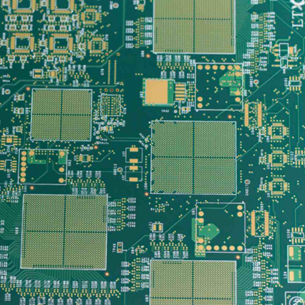
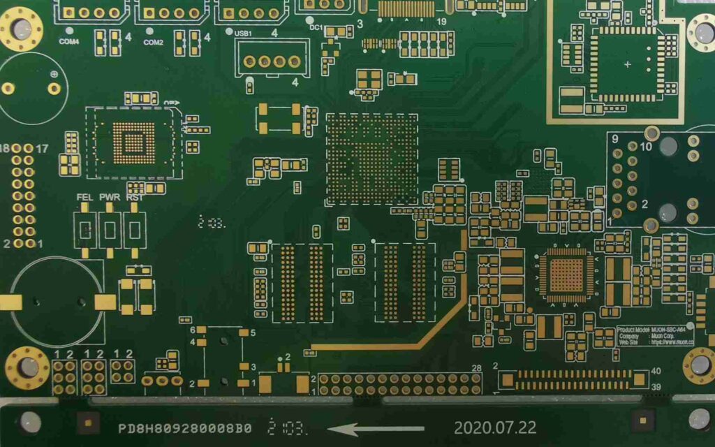
High-density interconnect (HDI) printed circuit boards (PCBs) are an advanced PCB technology that enables higher circuit densities than conventional PCBs. HDI PCBs have increasingly become the standard in mobile devices, wearables, automotive electronics, aerospace applications and other products where high functionality is required in a compact form factor.
Some key characteristics of HDI PCBs:
- Extremely dense interconnects: More routing channels and smaller spacing/line widths of traces (e.g. 2-5 mil line and space)
- Thinner dielectric layers: Typically using dielectric materials like polyimide in thicknesses of ~1.5 to 4 mils
- Microvias: Small vias with diameters typically 6 mils or less connecting layers
- Multiple lamination stages: Complex layer stackups with staggered vias
HDI technology allows packing of more components and connections in a given PCB footprint area. This article provides an overview of HDI PCB technology, processes, design considerations and applications.
Benefits of Using HDI PCBs
Here are some of the top benefits that HDI PCBs provide compared to conventional PCBs:
- Higher component density and interconnect density
- Miniaturization – Fit more functionality in smaller electronics packages
- Enable advanced, compact product designs
- Improve electrical performance through shorter traces
- Faster signal speeds through thinner dielectrics
- Reduce noise coupling by containing signals in a small area
- Facilitate RF designs and high-speed digital circuits
- Allow flexible/rigid-flex designs with dynamic flexing regions
- Accommodate high pin-count components like BGAs
In short, HDI PCB fabrication technology makes it feasible to develop electronic products that are lightweight, feature-packed, high-performance and compact. HDI capabilities enable innovation in product miniaturization across many end products.
HDI PCB Fabrication Process Flow
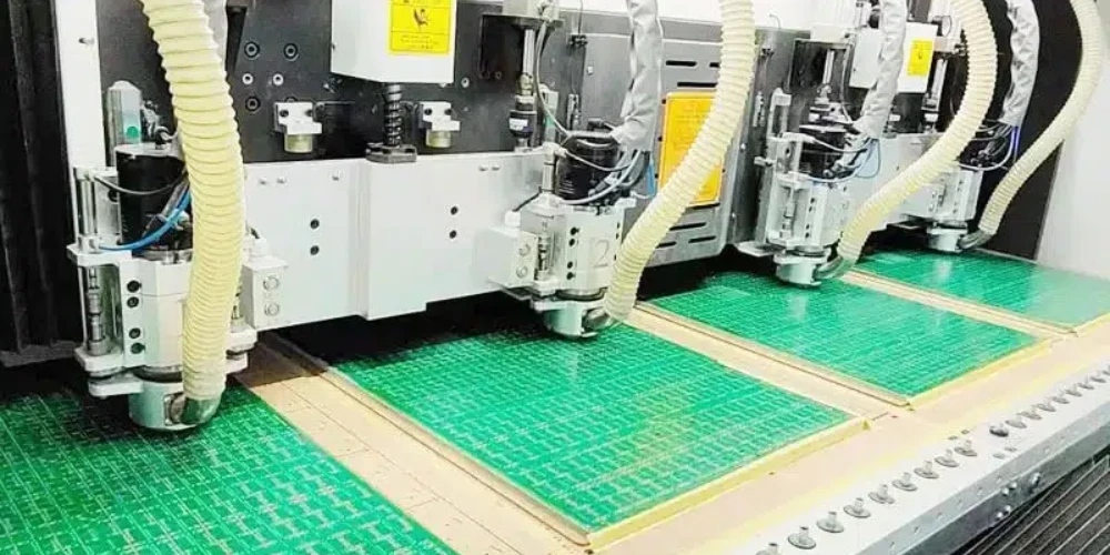
Fabricating HDI PCBs requires additional steps compared to conventional PCBs, due to the multilayer constructions and use of microvias. Here is an overview of a typical HDI PCB fabrication process flow:
1. Inner Layer Formation
- Create copper foil layers on dielectric substrates (polyimide, FR-4, Rogers, etc.)
- Photoimage and etch to form designed Cu traces and openings
- Plate copper in dielectric openings to form interconnect vias and through-hole vias
- Repeat processes to build up multiple HDI layers aligned with drilled blind vias
2. Outer Layer Processing
- Build up outermost circuitized layers on top and bottom surfaces
- Pattern solder mask and legend inks on outer layers
3. Layer Alignment and Bonding
- Use advanced alignment equipment to align layers and minimize registration errors
- Bond layers together using high temperature and pressure while curing dielectric adhesives
4. Microvia Formation
- Use laser drilling, plasma etching or photolithographic patterning to create microvias
- Metallize microvia walls using copper electroless and direct plating
- Electrolytic copper plate to build up microvia interconnects
5. Final PCB Finishing
- Electrical testing of circuits
- Surface finish plating – immersion gold, ENIG, etc.
- Route individual PCBs from panel
- Quality inspection and functional testing
This multi-step process results in an HDI PCB with very fine features capable of high-density interconnections. Precision fabrication processes are required to manufacture these complex PCBs.
HDI PCB Design Guidelines
Designing a PCB using HDI technology requires some key considerations:
Layer Stackup
An HDI stackup has staggered microvias between thin core dielectric layers. This allows trace routing between microvia pads, rather than being restricted to surface layers. Some example constructions:
- 4-layer HDI: Outer layers + 2 buried core layers connected by microvias
- 6-layer HDI: Outer layers + 4 buried layers with tiered microvias
- Additional core layers can be added for very complex designs
Using several thin core dielectric layers maximizes routing channels available. Common dielectrics include polyimide, PTFE composites, FR408 HR, and others. Core thicknesses are typically ~2 mils.
Trace Routing
With multiple thin core layers available, routing high density traces is enabled on internal layers. This reduces the reliance on outer layers for interconnections. Some guidelines:
- Use minimum trace/space widths between 2-4 mils on outer and inner layers
- Plan routing layers such that critical high-speed nets have minimal vias
- Use thin core layers to isolate or sandwich high-speed signals when needed
- Route differential pairs on same layer with controlled length and spacing
Component Land Patterns
Use minimum pad geometries sized for lead-free soldering requirements. Typical land diameters are:
- 0402 discrete pads: 0.6 to 0.8 mm
- 0.4 mm pitch QFN pads: 0.22 to 0.3 mm
- 0.5 mm pitch BGA pads: 0.25 to 0.3 mm
- MicroBGAs may allow 0.15 to 0.2mm pads
Ensure pad shapes and spacing account for solder mask web tolerances.
Microvias
Microvias with a diameter of 6 mils or less interconnect HDI layers. Laser drilled or photo-patterned microvias allow connections from an inner core layer to outer layers.
- Place microvias in pads or anti-pad clearance areas, not under traces
- Ensure sufficient annular ring for plating reliability
- Stagger adjacent microvias across layers to avoid weak spots
lamination
Using thinner dielectric core layers enables very high laminate densities, but increases challenges for controlling layer-to-layer registration during bonding. Tight registration tolerances are specified for HDI designs.
HDI PCB Applications
Some examples of products using HDI PCBs:
Consumer Electronics
- Smartphones
- Tablets and notebooks
- Wearable devices
- Digital cameras
Automotive Electronics
- Engine control units
- ADAS modules
- Infotainment systems
Aerospace and Defense
- UAVs, drones and avionics systems
- Radar and satellite payloads
- Missile guidance systems
Medical Devices
- Implantable devices
- Hearing aids
- Wearable patient monitors
IoT Devices
- Wireless router boards
- Compact sensor modules
- Wearable technology
The miniaturization and performance requirements in these applications drives the need for HDI PCB capabilities.
Here is a comparison of some key characteristics in a typical HDI PCB versus standard density PCB:
| Parameter | Standard Density PCB | HDI PCB |
|---|---|---|
| Dielectric Thickness | 5-10 mils | 1.5 – 4 mils |
| Line Width/Space | ≥ 6 mil | 2 – 4 mil |
| Via Diameter | ≥ 8 mil | ≤ 6 mil |
| Pad Size | ≥ 0.6 mm | 0.2 – 0.3 mm |
| Routing Layers Used | ≤ 6 Layers | ≥ 6 Layers |
HDI PCB Design and Analysis Tools
To facilitate the design of complex HDI PCBs, CAD tools provide extensive features for trace routing, 3D modeling, constraint checks and signal analysis. Here are some key capabilities:
- Real-time design rule checks during routing
- Microvia and backdrill automation
- Extensive stackup planning tools
- Flexible, high-speed tuning routing
- Length matching for differential pairs
- 3D view of PCB with embedded components
- Rigid-flex layer shapes and bending analysis
- Electrical rule checking on signal timing, noise, EMI
- DFM validation of manufacturability
- Thermal analysis of component thermal zones
- Modeling of power delivery network impedance
Advanced PCB design flows enable engineers to take full advantage of HDI fabrication capabilities and implement miniaturized, high performance products.
HDI PCB Challenges and Considerations
While HDI technology provides many benefits, the design and fabrication process also comes with some inherent challenges:
- Tighter tolerances required on trace geometries and registration
- Fabrication processes are more complex and costly
- Testing and inspection requires advanced X-ray tools
- Repair and rework is extremely difficult
- High-volume production needs strict process controls
- Thermal management is critical with high-power components
- Modeling and analysis of electrical performance is essential
- High-frequency design practices must be followed for signal integrity
- HDI design expertise required for complex layer stackups
- Separation of high-speed routes and grounds is tricky
With careful design techniques, analysis validation and tight process controls, these challenges can be effectively managed. Partnering with an expert HDI PCB manufacturer is recommended to achieve a robust, high-yield production flow.
Costs Analysis
Here is a comparison of approximate costs between standard and HDI PCBs:
| PCB Type | 6 Layer PCB | 10 Layer HDI PCB |
|---|---|---|
| Board Thickness | 1.6mm | 1.0mm |
| Minimum Line Width | 6 mil | 2 mil |
| Layer Count | 6 metal layers | 10 metal layers |
| Unit Cost Range | $80 – $250 | $250 – $1000 |
| Main Cost Drivers | Number of drilling steps and panel utilization | Thin dielectric materials, microvias, complex lamination process |
In summary, HDI PCBs range from 2X to 5X more expensive than standard multilayer boards due to the advanced materials and fabrication processes involved. But the benefits in miniaturization, performance and function integration offset the higher costs in many products.
Summary of HDI PCB Benefits and Applications
- Enables electronics miniaturization and innovation in many end products
- Ideal for advanced circuits in smartphones, IoT devices, automotive, aerospace, medical and more
- Provides highest interconnect density of any PCB technology
- Allows high component density and routing channels
- Facilitates high-speed circuit designs
- Polyimide-based constructions offer excellent thermal stability
- Complex HDI designs with 10-20+ layers are achievable
- Provides a path to even smaller microvias and traces in future
HDI PCB technology will continue advancing to meet needs for further miniaturization, higher speeds and greater reliability. This makes HDI PCBs central to many leading-edge electronic product designs.
FAQ
What are some key terms used with HDI PCBs?
Microvias – Small vias typically less than 6 mils diameter used to interconnect layers.
Sequential lamination – Method of bonding several thin dielectric cores together in multiple stages.
Staggered vias – Offset arrangement of vias from layer to layer to maximize connections.
Build-up layer – Additional thin dielectric and copper layer pair added to the main multilayer stackup.
Blind via – Hole and connection that extends through one layer without going fully through the entire PCB.
Buried via – An interconnect via that starts and ends within the middle layers of the PCB.
How are microvias formed in HDI PCBs?
There are three main methods to produce laser drilled microvias:
- Laser drilling – A CO2 laser pulses to ablate openings in each dielectric core layer. This is the most common and cost-effective approach.
- Plasma etching – Uses plasma to etch microvia openings. Provides excellent dimensional control.
- Photo-via – Lithographic patterning of microvias. Highest precision but also most complex process.
What design factors affect HDI PCB fabrication yield?
Some key design considerations for maximizing HDI PCB fabrication yield:
- Allow sufficient annular rings on microvias for reliable plating
- Follow minimum spacing rules between microvias
- Ensure adequate anti-pad clearance sizes for density requirements
- Limit the number of lamination steps for layer stackup
- Use designs supported by modeling, analysis and DFM checks
- Partner with manufacturer early to assess design manufacturability
How are HDI PCBs tested and inspected?
Testing HDI PCBs requires advanced inspection tools due to the microvia structures and high density:
- Automated optical inspection (AOI) checks external layers
- 2D and 3D X-ray scans verify internal boards structure
- Automated test systems validate electrical connectivity
- Flying probe testing detects shorts and opens
- Additional functional testing may be implemented
Rigorous inspection regimes ensure reliability and early detection of any defects.
What are the limitations of HDI PCB technology?
Some inherent limitations to current HDI PCB technology include:
- Minimum microvia diameters approaching 2 mils
- Trace/space widths approaching 1 mil
- High frequency signal loss and skew issues
- Component warpage stresses with high density mounting
- Thermal dissipation for high power components
- Complexity limits manufacturability at leading edge
- Costs increase exponentially with added layers and density
Ongoing advances in materials, processes and design tools continue to push the limits of HDI PCBs further.


Leave a Reply