Introduction
High-density interconnect (HDI) multilayer PCBs have become increasingly popular in recent years due to the growing demand for smaller, lighter, and more powerful electronic devices. HDI PCBs allow for greater component density by utilizing thinner dielectric materials and finer lines and spaces. They enable more interconnects and layers in a given footprint area compared to conventional PCBs. This article will provide an in-depth look at HDI multilayer PCB technology, including its key benefits, critical design considerations, and advanced manufacturing processes.
What are HDI Multilayer PCBs?
HDI PCBs refer to printed circuit boards with higher wiring densities than conventional PCBs. They contain multiple stacked layers with very fine traces and spaces of 6 mils or below. HDI PCBs utilize dielectric materials that are thinner than standard laminates, with dielectric thicknesses starting at 3 mils or below. This allows routing traces closer together horizontally and stacking more circuit layers vertically while maintaining a thinner overall board thickness.
Some key characteristics of HDI multilayer PCBs:
- Trace/space of 6 mils or below
- Thinner dielectric layers (3 mils or below)
- High layer count (12-30+ layers)
- Laser drilled microvias (5-10 mils)
- Fine line geometries (5/5um line/space)
- Higher interconnect density
- Overall thinner board thickness
HDI technology enables several circuit layers to be consolidated into a single PCB, reducing the overall footprint size. The finer geometries and thinner dielectrics allow for shorter, more optimized routing paths. This is critical for many space-constrained and high-speed designs.
Benefits of Using HDI Multilayer PCBs
There are several key benefits that make HDI multilayer boards an attractive option:
Size Reduction
- Thinner dielectric materials and smaller traces/spaces allow for a more condensed board layout in a smaller physical footprint. This enables miniaturization of electronics.
Increased Routing Channels
- The ability to stack more circuit layers with thinner dielectrics provides more routing channels. This facilitates complex routing and higher connection densities.
High-Speed Performance
- Finer geometries enable improved high-frequency response. Shorter distances between components reduce signal loss and propagation delays.
Noise Reduction
- Additional ground planes help isolate signals and contain noise/cross-talk. This improves signal integrity at high frequencies.
Weight Reduction
- A greater number of circuit layers can be packed into an overall thinner board profile, reducing weight. This is advantageous in weight-sensitive applications.
Improved Reliability
- Laser drilled microvias offer better connection reliability than through-hole vias. The reduced via pitch also enables more redundant connections.
Design Flexibility
- HDI provides more freedom and flexibility in routing complex, high-density designs. Microwave designers also leverage HDI’s benefits.
In summary, HDI PCB technology enables smaller, lighter, faster, and more functional PCBs vital for the latest electronic devices and systems. The tradeoffs are higher costs and more complex design/manufacturing requirements.
HDI Multilayer PCB Design Considerations
While HDI multilayer PCBs offer significant advantages, they also pose some unique design challenges:
Signal Integrity
- With traces in very close proximity, maintaining signal integrity is critical. Proper stackup planning, routing practices, and simulation are required.
Thermal Management
- More layers and higher densities lead to increased thermal loads. Thermal analyses and planning for heat dissipation are necessary.
Materials Selection
- Thinner dielectrics require special laminate materials with suitable properties. Glass reinforcement and coefficient of thermal expansion (CTE) are important considerations.
Registration/Tolerances
- Tight tolerances are maintained during lamination to enable forming interconnections between layers. This requires strict process controls.
Via Reliability
- Laser drilled microvias must have sufficient land diameters and plating thickness to ensure reliability under thermal/mechanical stresses.
Component Selection
- Components must be suitable for fine pad/pitch footprints and reflowing. BGAs, 0201 and 01005 discrete passives are common.
Testing/Inspection – Testing for opens/shorts during fabrication requires specialized flying probe or x-ray inspection tools due to fine feature sizes.
Proper planning to address signal and power integrity, thermal design, manufacturability, and reliability are necessary when designing HDI PCBs. Close coordination with the PCB fabricator is highly recommended.
HDI PCB Stackup Considerations
The layer stackup is a critical consideration when designing HDI multilayer boards. Some key guidelines:
- Place ground layers adjacent to signal layers to provide shielding and isolation. Use several thin dielectrics rather than one thick layer.
- Maintain symmetry from the center of the board to balance stresses and avoid warpage.
- Alter signal layer order orthogonally (e.g. sig-gnd-pwr-gnd-sig-core-sig-gnd-pwr-gnd-sig) to further contain signals.
- Keep layer count below 30 layers due to diminishing returns on density versus complexity.
- Place heavily routed layers on the outer third of the stackup to simplify via transitions.
- Define impedance-controlled routing layers to maintain consistent transmission line properties.
Proper HDI stackup design prevents signal degradation while optimizing routing density, thermal conduction, and manufacturability. Modeling and simulation verifies the stackup before manufacturing.
HDI PCB Design and Layout Considerations
In additional to the stackup, designing and laying out HDI PCBs also requires special considerations:
- Use smaller component footprints with finer pad/pitch spacings such as 0201 or 01005 discretes.
- Leverage blind/buried vias for layer transitions rather than through-hole vias to save space.
- Use grid sizes of 5 mils or below for routing traces. Observe minimum trace widths based on current.
- Verify trace impedance matches system requirements. Controlled impedance routing is recommended for high-speed signals.
- Avoid 90° trace corners. Use arcs or mitered corners to reduce impedance discontinuities.
- Establish design rules for length matching, crosstalk, and coupling to ensure signal integrity. Simulate and verify routing.
- Allow for thermal relief cutouts, thermal vias, and/or copper balancing where necessary.
HDI design requires tight constraints, attention to signal integrity, and advanced layout skills to fully utilize the technology. Rigorous validation of the design is strongly advised.
HDI PCB Microvia Fabrication Process
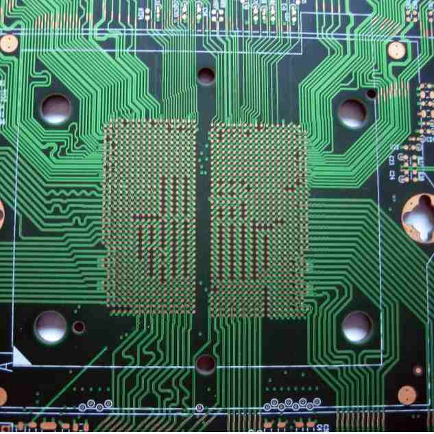
HDI PCBs use microscopic vias called microvias for the interconnects between layers. This is a brief overview of the microvia fabrication process using laser drilling:
1. Imaging – Photoresist is applied and imaged to define the pads for the microvias.
2. Laser Drilling – A CO2 laser drills holes through the pads in the exposed dielectric. Typical microvia diameters range from 5-10 mils (0.13-0.25mm)
3. Desmear – The via holes are cleaned of debris and given a chemical etch to remove smeared resin.
4. Metallization – The microvia holes are plated with copper to form the electrical connections between layers. Minimum 25um plating is typical.
5. Imaging – Photoresist is applied and imaged to define the pattern for traces and pads on the layer.
6. Copper Etching – Unwanted copper is chemically etched away, leaving only the desired conductor pattern.
7. Strip Resist – Photoresist is stripped away, leaving finished conductors with plated microvias.
Repeat process for each layer, accurately aligning the layers, to build up a multilayer HDI PCB with high interconnect density.
HDI PCB Panelization and Assembly
To maximize manufacturing efficiency, PCB fabricators produce HDI boards in panel form containing multiple PCBs:
- Individual PCBs are arranged in a square panel for compatibility with fabrication equipment.
- Panels may contain v-scoring or rout paths to facilitate separating boards.
- Fiducial markings on panels aid in layer-to-layer alignment during lamination.
- Panel sizes (18”x24”, 21”x24”, etc.) are optimized for equipment and to minimize waste.
- Component placement software supports panelized assemblies to leverage panel manufacturing.
- PCB assembly equipment can populate full panels of boards prior to depaneling.
Panelizing HDI multilayer boards provides throughput and efficiency benefits compared to processing individual boards. Assembly as panels also improves productivity.
Summary of Key Points
- HDI multilayer PCBs enable increased routing density with fine lines/spaces and high layer counts.
- Key benefits include miniaturization, improved high-speed performance, noise reduction, and design flexibility.
- HDI PCB design requires attention to signal/power integrity, thermal design, tolerances, and component selection.
- Stackup construction and layer sequencing techniques help optimize HDI designs.
- Microvias created with laser drilling provide reliable interconnections between the many layers.
- Panel-based fabrication and assembly improves manufacturing throughput of HDI boards.
- While more complex to design and manufacture, HDI multilayer technology delivers significant advantages for advanced PCBs.
Frequently Asked Questions
Here are some common FAQs regarding HDI multilayer PCB technology:
Q: What are the minimum trace/space and dielectric thicknesses for a PCB to be considered HDI?
A: Traces and spaces of 6 mils or below on dielectric layers of 3 mils or thinner would classify a PCB as HDI. However, more advanced HDI may use traces below 5 mils on dielectrics less than 2 mils thick.
Q: Can conventional through-hole components be used on HDI boards?
A: It is recommended to use only surface mount components, particularly finer pitch packages, to match the capabilities of HDI boards. Through-hole parts are discouraged but may be used selectively if space allows.
Q: What are the typical layer counts for HDI multilayer boards?
A: While dependent on design complexity, HDI boards typically range from 12-30 layers. More than 30 layers is possible but becomes challenging in terms of manufacturability and cost. High-end networking or telecom boards may utilize 70+ layers in some cases.
Q: How are HDI PCBs tested and inspected during fabrication?
A: Flying probe electrical testing and x-ray inspection tools are commonly used. Automated optical inspection (AOI) can be implemented for process quality control of finer features.
Q: What design software tools support HDI PCB layout and routing?
A: Many leading PCB design packages support HDI design rules, blind/buried vias, and high layer counts. These include Cadence Allegro/OrCAD, Mentor Graphics Xpedition, and Altium Designer. Signal integrity simulation is also advised.
References
IPC-2226A Sectional Design Standard for High Density Interconnect (HDI) Printed Boards
“The HDI Handbook” by Donald Ostermann, Happy Holden
“High Density Interconnect PCB Technology Overview” – Z-zero
“Are Microvias Reliable for HDI?” – EIPC Conference 2007
“HDI Stack Planning: Critical Aspect of HDI” – PCBDesign007


Leave a Reply