In the world of printed circuit boards (PCBs), high-density interconnect (HDI) PCBs with microvias are becoming increasingly popular for their ability to accommodate more complex circuitry in a smaller space. HDI microvia PCBs provide numerous benefits over traditional PCB technologies, making them well-suited for advanced electronics and devices where space, weight, and performance are critical factors.
What are HDI Microvia PCBs?
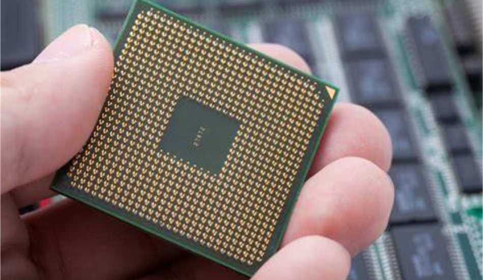
HDI PCBs use thinner dielectric material and trace/space widths, allowing for a denser interconnection of components on the board. Microvias are small vias that connect different layers in an HDI PCB stackup. Traditional PCBs use through-hole vias with larger diameters to connect layers. By contrast, HDI microvias have diameters less than 150 microns, allowing connections between layers in a PCB without taking up as much space.
The combination of thinner dielectrics, finer lines and spaces, and microvias gives HDI PCBs their high density advantage. More interconnects can be routed in the same area, increasing wiring capacity. Microvias also provide connections between layers that minimize layer-to-layer distances, improving high-speed signal integrity.
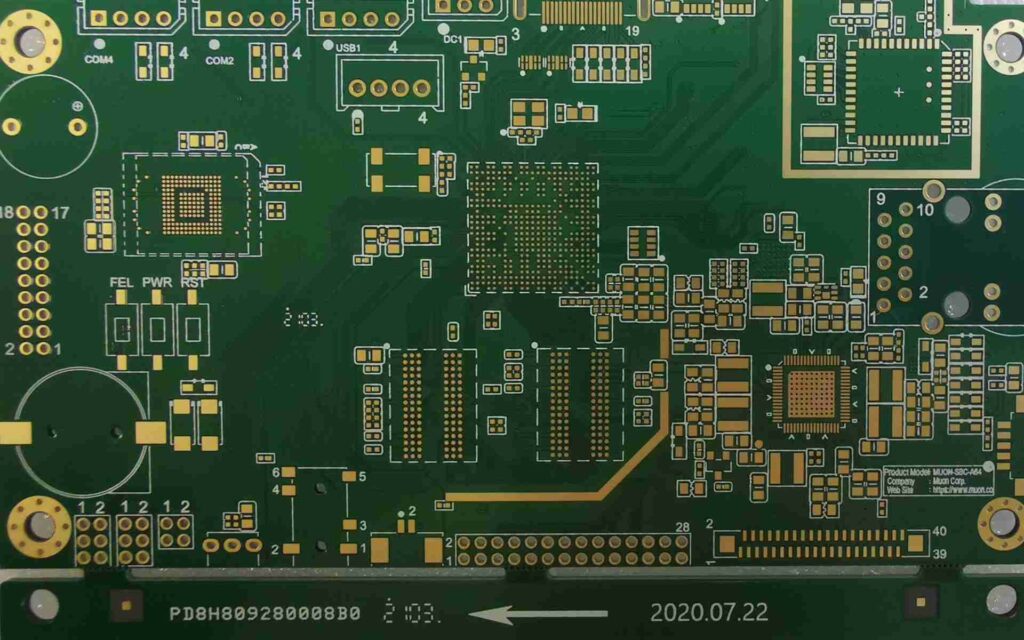
HDI PCB Stackup
A typical HDI PCB stackup contains more layers than a conventional PCB. This might include:
- Outer layers with finely spaced traces for component interconnects
- Two or more thin core dielectric layers, each with traces on both sides
- Multiple layers of microvias for vertical interconnections between layers
- Power and ground planes to provide power integrity
- Signal layers with controlled impedance traces for high-speed signals
- Solder masks and silkscreens for component placement and identification
The layers are aligned precisely, laminated, and pressed together to form a unified board. The result is a dense, multilayer structure capable of handling complex circuits.
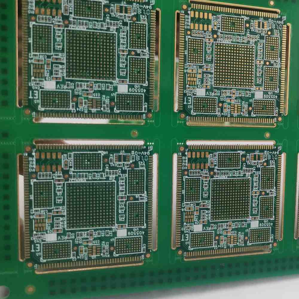
Microvia Properties
Microvias in HDI PCBs have the following characteristics:
- Diameters less than 150 microns, typically 50 to 100 microns
- High aspect ratios up to 10:1 (via depth to diameter)
- Plated along the interior walls to form conductive connections
- Filled with epoxy or other materials to support thin core dielectric layers
- Laser drilled or photo-processed openings
The small diameter maximizes PCB surface utilization while the high aspect ratio provides connections between multiple layers. Advanced drilling and plating technology are required to produce quality microvias.
Benefits of Using HDI Microvia PCBs
HDI microvia PCBs offer several key advantages that make them an attractive option for many advanced circuit designs:
Space Savings
By utilizing thinner dielectrics, finer traces, and microvias, HDI PCBs can accommodate more interconnects per unit area. This space savings allows for:
- Denser component placement
- More routing channels for traces
- Compact layout of high I/O devices like FPGAs
- Miniaturization of end products
The space savings are substantial compared to conventional PCBs. HDI PCBs take full advantage of their Z-axis space to maximize circuit density.
Signal Integrity
With their multiple thin dielectric layers and microvias, HDI PCBs enable shorter traces between ICs and other components. The shorter layer-to-layer distances reduce noise and propagation delay, improving signal integrity for high-speed signals. Transmission speeds up to 20+ Gbps can be realized with careful HDI stackup design.
Microvias provide vertical connectivity while avoiding lengthy trace lengths. Optimized ground/power planes also enhance signal integrity through controlled impedance environments for traces.
Reliability
Despite their complexity, HDI microvia PCBs achieve high reliability due to stringent design rules and manufacturing processes. Factors supporting reliability include:
- Stringent drilling/plating processes produce quality microvias
- Thin core dielectrics reduce stress compared to thick cores
- Glass cloth in core layers provides dimensional stability
- Epoxy via fill prevents layer separation or cracking
- Careful stackup design minimizes thermal stresses
HDI PCBs avoid many traditional PCB failure points like via cracking or plating separation. Proper design and fabrication is critical to realize reliability advantages.
lightweight
By utilizing thinner dielectric layers and eliminating non-functional copper, HDI PCBs can achieve substantial weight reductions compared to conventional designs. This helps reduce the weight of end products, which is especially beneficial in aerospace, defense, and portable electronics applications.
The potential to integrate circuits in less PCB layers results in fewer laminated copper/dielectric layers overall. And the microvias themselves take up almost no weight compared to through-holes. Every bit of reduced weight counts when optimizing products for minimum size and weight.
Applications of HDI Microvia PCBs
With their unique benefits, HDI microvia PCBs are commonly used in the following types of advanced electronic systems:
Consumer Electronics
Cell phones, tablets, notebooks, wearables, IoT devices, and other interconnected consumer electronics demand maximum functionality in minimum footprints. HDI PCBs help pack more computing power and features into amazingly small products.
Automotive Electronics
Automotive applications like engine control units (ECUs), driver assistance systems, and in-vehicle infotainment rely on dense, high-reliability PCBs. HDI microvia boards meet automotive reliability standards while providing space savings.
Medical Electronics
Medical devices like patient monitors, imaging systems, and implanted devices need reliable, high-density PCBs. HDI microvia technology supports complex medical electronics in tight spaces.
Aerospace/Defense
Avionics, guidance systems, and other mission-critical military electronics operate under extreme conditions. Ruggedized HDI PCBs deliver aerospace-grade performance at reduced size and weight.
High-Speed Communications
Data centers, networking gear, 5G infrastructure, and other communications applications demand maximum throughput. HDI PCBs provide the signal integrity and space savings needed for high-speed communication systems.
In general, any application where reliability, signal integrity, and space utilization are important factors can benefit from HDI microvia PCB technology. The tradeoffs are higher fabrication costs and design complexity compared to conventional PCBs.
HDI Microvia PCB Design Considerations
Designing a high-quality HDI microvia PCB requires attention to the following factors:
Stackup Design
The layer stackup must balance signal isolation needs, impedance control, power delivery, and manufacturability. Important aspects include:
- Number of layers and definitions
- Order/function of layers
- Dielectric materials and thicknesses
- Plane layers for power integrity
- Placement of controlled impedance layers
- Total board thickness
Simulation and analysis tools like HyperLynx can optimize the stackup early in the design flow.
Routing Architecture
Efficient routing architectures utilize the Z-axis space of HDI PCBs while meeting signal integrity constraints. This may involve:
- Grid-based topologies for BGA escape routing
- Restricted zones for controlled impedance signals
- Non-functional pads/vias for layer transitions
- 3D visualizations to optimize layer usage
Component Placement
IC and component placement must align with board space utilization needs and the routing architecture. High pin count devices may require multiple rows or perimeter array patterns.
Materials Selection
The choice of dielectric, copper, and other materials impacts manufacturability. Factors like coefficient of thermal expansion (CTE) mismatches and process compatibility need to be evaluated.
Design Rules
HDI PCB layout tools must account for manufacturable design rules on trace/space, hole sizes, routing angles, plane connections, and other physical design elements. Both electrical and fabrication constraints need to be followed.
Following established HDI design practices will help avoid pitfalls and achieve a first-pass design success. Reference designs from the fabricator are also useful at the start of a new HDI PCB project.
Summary of HDI Microvia Benefits
The combination of HDI and microvia technologies provides the following advantages that are driving adoption across many industries:
- Dramatic space savings compared to conventional PCBs
- Improved signal integrity for high-speed digital systems
- Increased interconnect density for complex ICs and devices
- Weight reduction important for portability
- Reliability equal to or better than standard PCBs
- Enables miniaturization and improved performance
As electronic devices continue getting smaller while packing more functionality, HDI microvia PCB technology enables this continue progress. With sound design practices, even the most demanding space and performance requirements can be met. While fabrication costs are higher than standard PCBs, the benefits are often well worth the investment for advanced circuit applications.
Frequently Asked Questions
What are the typical design rules for microvias?
Typical design rules include minimum microvia diameter of 50 microns, minimum drill diameter of 40 microns, and via pad sizes ranging from 80 to 150 microns depending on the via size. High aspect ratio microvias have a typical depth to diameter ratio of 8:1 to 10:1.
How are microvias formed in the PCB fabrication process?
Microvias are either laser drilled or photo-processed in the core and build-up dielectric layers. The holes are plated with copper to form the interlayer connections. Filling of the remaining hole with resin prevents layer separation.
What are the limitations of microvia technology?
The main limitations are the fabrication complexity and cost compared to standard PCBs. Designers also face more complex design rules and stackup considerations. Maximum board thickness is limited by what lamination presses can process.
How do you test for reliability of microvias?
Microvia reliability testing often includes temperature cycling, vibration testing, and inspecting micro-sections of vias for signs of cracks or failures. Automated optical inspection also checks for defects.
Can microvias be repaired if defective?
If testing reveals defective microvias, it is generally not possible to repair them without scrapping the PCB. This emphasizes the importance of robust design and fabrication processes to achieve high yields.
Conclusion
HDI microvia PCB technology enables highly advanced electronics and devices that could not exist without the space savings and performance provided. As demand grows for ever-smaller yet more capable devices across countless industries, HDI PCBs will continue seeing rapid adoption and innovation. While fabrication and design complexity remain challenges, the potential benefits make this a key technology moving forward for modern printed circuit boards.


Leave a Reply