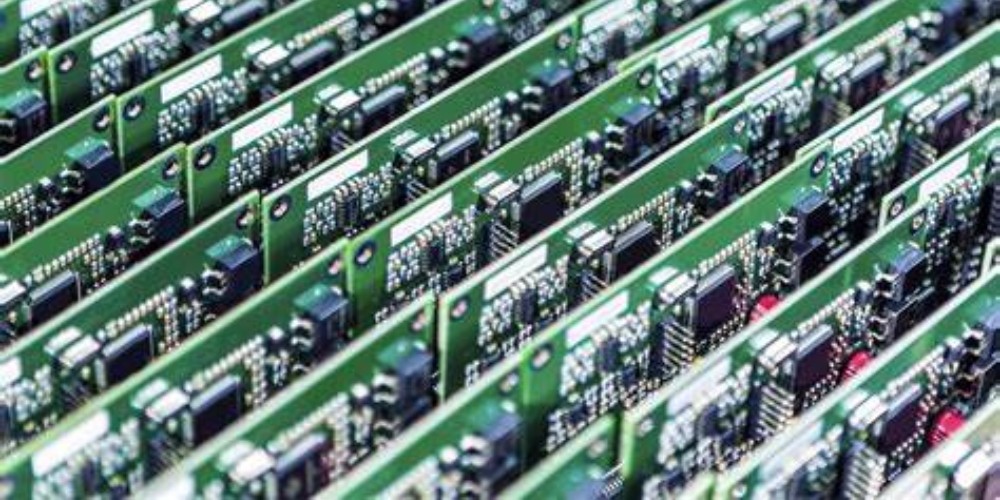
HDI (High Density Interconnect) is a advanced PCB (printed circuit board) manufacturing technology that allows the production of complex multilayer circuit boards with extremely high component density. The HDI process enables the fabrication of interconnects with trace widths and spacings down to 5/5 μm (micrometers), via diameters down to 50 μm and line/space of 10/10 μm. This enables a greater level of circuit miniaturization and integration compared to conventional PCB processes.
Overview of the HDI Manufacturing Process
The HDI manufacturing process involves several key steps:
HDI Substrate Creation
- The base material is a dielectric resin typically epoxy, polyimide or a blended resin engineered for HDI.
- The dielectric allows finer lines and spaces due to its high glass transition temperature, low Z-axis expansion and high modulus properties.
- Sheets of dielectric core material are laminated with sheets of copper foil.
Photolithography
- A layer of photoresist is applied on the copper surfaces.
- The resist is exposed to UV light through a photomask with the circuit pattern.
- Exposed areas are polymerized (negative resist) or depolymerized (positive resist).
- The resist is developed, selectively removing the unexposed (negative) or exposed areas (positive).
- The copper is etched away from the areas without resist, creating the circuit traces.
Laser Drilling
- Microvias are drilled through the dielectric using an excimer UV laser.
- Laser drilling can achieve 50μm diameter vias with high precision.
- Allows much higher via density compared to mechanical drilling.
Conductive Metallization
- The laser drilled vias are seeded and then electrolessly plated with copper to metallize the via barrels.
- Electroplating then deposits more copper, completely filling the vias.
- A chemical-mechanical polishing (CMP) step then removes excess plating, planarizing the surface.
Layer Buildup
- Additional alternating layers of dielectric and patterned copper can be stacked for complex HDI boards.
- More layers allow higher component densities.
- 4-16 layers is typical but >20 layers are possible.
- Stackup design is important for electrical performance.
Outer Layer Imaging
- Final photolithographic patterning of the outer layer circuitry on both sides of the HDI board.
Soldermask and Surface Finish
- A soldermask is applied to coat the board except at solderable pads.
- OSP, ENIG or other surface finishes are added to protect and facilitate soldering.
Final Processing
- Visual inspection and electrical testing confirms quality.
- Panels are routed into individual PCBs.
- Finished boards are shipped to customers.
Benefits of HDI Technology

There are several key benefits that make HDI the technology of choice for many advanced PCBs:
- Increased Routing Density – The fine features allow routing in extremely tight spaces not possible with standard processes. This enables greater miniaturization.
- Higher Component Density – More components can be packed onto HDI boards due to the routing capability.
- Improved Electrical Performance – The closely spaced ground planes and traces have improved impedance control for high speed signals.
- Reduced Layers – A 6-10 layer HDI board can replace a 18+ layer standard board, reducing costs.
- Enhanced Functionality – The multilayering provides more opportunities for embedded components and high density interconnects.
- Lower Weight and Volume – HDI allows electrical systems to have a smaller footprint and lower mass.
HDI Design Considerations
While offering advantages, HDI also has some important design considerations:
- Materials Selection – Dielectrics must have suitable properties to enable microvia laser drilling and fine feature photolithography.
- Stackup Design – Ground/power planes and signal routing layers must be intelligently arranged for electrical performance.
- Trace width/spacing – 5/5 μm lines/spaces impose constraints on current carrying capability and crosstalk.
- Via capture pads – Laser drilled microvias require capture pads. These constrain routing density in their vicinity.
- Aspect ratios – High density interconnects produce high aspect ratio traces and vias which impact manufacturability.
- Signal integrity – Simulations typically required to verify electrical performance due to tight geometries.
Typical End Products Using HDI
Some examples of advanced products manufactured using HDI PCB technology:
- Smartphones – HDI allows the high computing power and component density needed.
- Wearable technology – Miniaturized and flexible circuits for watches, fitness trackers, etc.
- Internet of things devices – Enables tiny but capable PCBs for networked sensors and devices.
- Medical devices – Allows electronic instrumentation to be compact and portable.
- Aerospace/defense – Rugged, lightweight and high reliability boards for extreme environments.
- Automotive – Used to integrate electronics and expand capabilities of modern vehicles.
- High speed computing – Provides interconnect capability for fast processors and memories.
As electronic devices continue advancing to provide more functionality in smaller packages, HDI will remain an essential enabling technology for many leading edge products and applications.
Frequently Asked Questions
What are the key differences between HDI and standard PCB fabrication?
The main differences are:
- Fine features – HDI can achieve trace widths/spacings down to 5/5 μm versus ~50/50 μm for standard processes.
- Microvias – HDI utilizes laser drilling to produce vias down to 50 μm diameter vs. 150 μm with mechanical drilling.
- Thin dielectrics – HDI uses dielectrics as thin as 50 μm versus >100 μm for standard PCBs.
- Higher layer count – HDI enables reliable production of boards with 12-20+ layers. Standard boards typically max out at 16 layers.
- Tighter tolerances – HDI holds tighter tolerances on line widths/spaces, hole sizes and layer alignment.
What are the key factors that enable the fine features of HDI?
There are three primary factors:
- Advanced dielectric materials engineered to enable laser drilling, thin cores, and fine lithographic patterning.
- Photolithography tools with very high resolution and precise imaging capabilities.
- Laser drilling tools such as the UV excimer laser which can create small vias with high precision.
How are microvias created in the HDI process?
HDI uses an excimer UV laser to ablate tapered holes through the dielectric material. The laser energy vaporizes material to penetrate the core. The laser beam is shaped and focused to produce the desired via profile and diameter, typically 50 μm. The laser drilling achieves high accuracy and repeatability for high density vias across the board.
Does HDI require special soldering processes?
In most cases HDI boards can be soldered using standard surface mount assembly processes. The use of laser microvias means there are no issues with solder wicking that can occur with plated through holes. For boards with very fine pitch devices, solder paste printing capability may need attention. Also, inspection tools may require higher magnification modes.
Can flex PCBs use HDI technology?
Yes, the HDI process can be implemented on flex circuit dielectrics like polyimide. This allows flex circuits to achieve very high interconnect densities. Careful material selection and stackup design is required to ensure the flex circuit can withstand the lamination pressures and temperatures involved. The result can be very tiny but extremely sophisticated flex circuits.


Leave a Reply