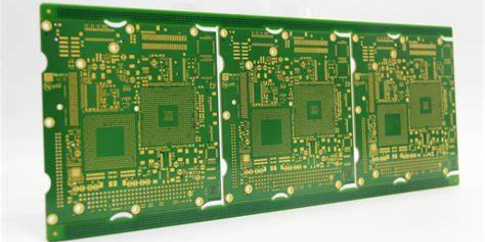
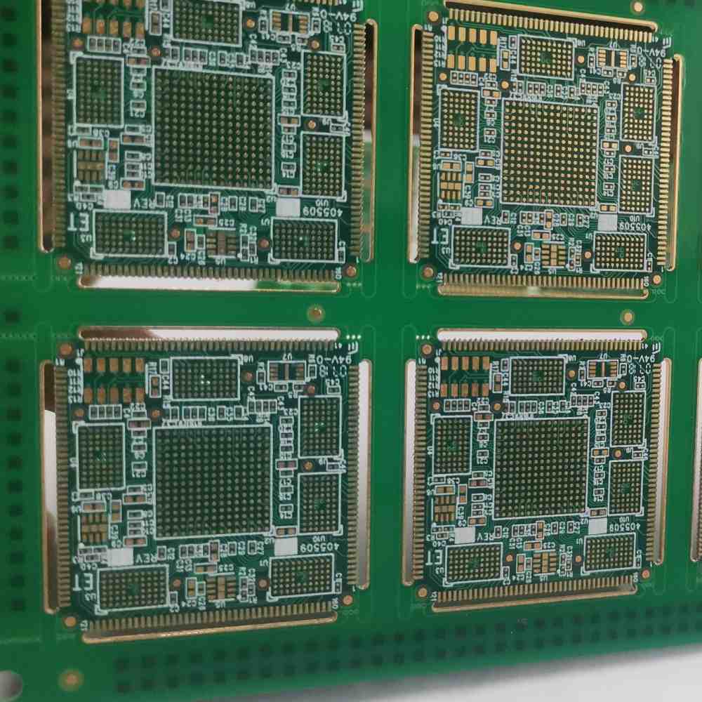
What is HDI in PCBs?
HDI (High Density Interconnect) is a PCB (Printed Circuit Board) technology that enables higher component density and more interconnects than standard PCBs. HDI allows for smaller features, finer lines and spaces, smaller vias, and higher connection pad densities.
HDI PCBs have several benefits compared to standard PCBs:
- More routing channels for traces
- Smaller overall PCB size
- Higher component density
- More flexibility in component placement
- Support for advanced packaging like BGAs
- Higher signal speed and quality
The key characteristics of HDI PCBs are:
- Line/space of 6/6 mil or smaller
- Microvias with diameters of 6 to 10 mils
- Stacked microvias for layer transitions
- Capture pads for improved routing density
- Thin dielectric buildup layers, typically 2 to 4 mils
Why Use HDI Technology?
There are several key reasons to use HDI technology in PCB design:
Enable Miniaturization
HDI allows for greater miniaturization of PCBs. The smaller features and spacing mean components and traces can be packed more densely. HDI enables reducing the overall footprint of a PCB circuit.
Support High-Pin Count ICs
Integrated circuits with high pin counts, such as FPGAs and microprocessors, require HDI to route all the connections. The fine lines and high interconnect density of HDI is necessary to wire these devices.
Preserve Signal Integrity
With very dense wiring, maintaining signal integrity is critical. HDI provides shorter route lengths and allows matched length differential pairs to be routed with accuracy. This ensures signal quality.
Reduce Layer Count
By utilizing microvias to transition between layers, HDI design can reduce the layer count compared to an equivalent standard PCB. Fewer layers lowers costs.
Enable Embedding Components
HDI methods permit passive components like resistors and capacitors to be embedded within the PCB structure. This further miniaturizes the design.
Improve Reliability
The materials used in HDI PCBs are engineered for reliability under thermal cycling. This includes the dielectric buildup layers. HDI PCBs can meet reliability requirements under harsh operating conditions.
Support High-Speed Design
With precise differential pairs and contained return paths, HDI boards provide a superior high-speed platform for multi-gigabit data rates. HDI is a requirement for many high-speed applications.
HDI Design and Fabrication Overview
There are some key design and fabrication steps unique to HDI PCB technology:
1. Base Material Selection
The base laminate materials must have a low coefficient of thermal expansion (CTE) to withstand high density assembly and operation. Common materials are FR-4, polyimides, and PTFE composites.
2. Sequential Lamination
The dielectric buildup layers are added one at a time in an automated process of lamination, drilling, and copper plating. Construction is done in a sequential manner.
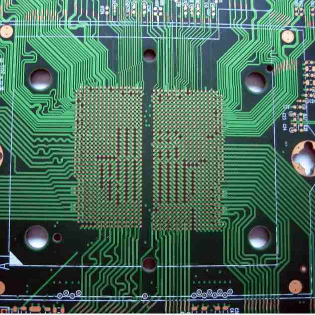
3. Microvias
Microvias with 6 to 10 mil diameters interconnect the buildup layers. These are drilled and plated before each additional layer. Stacking microvias connects signals between non-adjacent layers.
4. Thin Dielectrics
The dielectric buildup layers are much thinner than base laminate, typically around 2 to 4 mils thickness. This allows for fine lines and spaces.
5. Capture Pad Design
Capture pads are an enlarged area connected to a microvia specifically for routing traces. This improves routing density.
6. Fine Line Width/Spacing
Line width and spacing on HDI layers approach the capabilities of the fabricator, typically 6/6 mil or 5/5 mil. This sets HDI apart from standard PCBs.
7. Surface Finishes
A combination of selective gold plating and organic solderability preservatives (OSP) are typically used. This balances cost while providing solderability.
Here is a comparison of standard PCB and HDI PCB features:
| Feature | Standard PCB | HDI PCB |
|---|---|---|
| Line Width/Spacing | 8/8 mil | 6/6 mil or 5/5 mil |
| Dielectric Thickness | 14-28 mils | 2-4 mils |
| Microvia Diameter | 10-20+ mils | 6-10 mils |
| Capture Pad Size | N/A | 10-20 mils diameter |
| Via Process | Single step drill/plate | Sequential buildup process |
| Routing Layers | Any layer | On buildup layers only |
This summarizes the key technology differentiators that enable HDI PCBs to achieve high density interconnections.
HDI Design Guidelines and Layout
To effectively implement HDI in your PCB design, there are some layout guidelines to follow:
Partition the Circuitry
Partition components and nets onto specific PCB areas. This clustering localizes signals and constrains routing to a defined region, preventing interference.
Utilize a Grid
Use a fine grid for routing, such as 25 microns. This enables accuracy in trace widths and clearances to meet fabricator capabilities.
Budget Space for Microvias
Leave adequate space around microvias for capture pads and routing lines. A 10 mil microvia may need 15 mils x 15 mils or more of total area.
Stack Microvias Properly
Stack microvias over adjacent pads on different layers for optimal via placement. Stacking directly over one another risks misregistration.
Maintain Return Paths
Keep return paths on adjacent layers to minimize loop inductance. This prevents EMI and maximizes signal quality for high-speed signals.
Use Plane Layers
Incorporate plane layers for power, ground and signals. Solid planes provide shielding and controlled impedance environments for traces.
Follow Length Matching Rules
Match differential pair lengths within a tight tolerance, such as under 10 mils of variance. This prevents skew between differential signals.
Adhering to these guidelines will result in an HDI design that meets performance objectives while being manufacturable.
Here are some example HDI stackups:
4-Layer HDI Stackup
| Layer | Function |
|---|---|
| 1 | Signal Routing |
| 2 | Ground Plane |
| 3 | Power Plane |
| 4 | Signal Routing |
- 2 HDI layer pairs for routing
- Sandwiched between ground/power planes
- Thin dielectrics permit fine features
- Microvias provide dense vertical connections
6-Layer HDI Stackup
| Layer | Function |
|---|---|
| 1 | Signal Routing |
| 2 | Ground Plane |
| 3 | Power Plane |
| 4 | Signal Routing |
| 5 | Ground Plane |
| 6 | Signal Routing |
- 4 HDI layers for routing
- Additional power integrity with 3 planes
- Microvia transitions through all layers
- High density component placement on surface
HDI Design Challenges
While HDI offers many benefits, it also poses some design and fabrication challenges:
Meeting Trace Width/Spacing Rules
Achieving 5/5 mil or 6/6 mil trace/space requires strict design practices and advanced PCB equipment. This is at the leading edge of capability.
Generating Accurate Stackups
With multiple thin dielectric layers, ensuring proper stackup thicknesses and minimizing skew is critical for signal quality.
Achieving Acceptable Yields
Due to tight tolerances, HDI fabrication yields tend to be lower on initial runs as processes mature. There can be more rework.
Debugging Without Vias
Lack of probing vias on inner layers makes verifying inner layer signals difficult. X-ray tools are often needed.
Tuning For EMI Control
HDI circuits can require additional tuning measures for EMI control given the high component density. Attention to grounding is key.
Managing Thermal Loads
The concentrated heat from dense ICs and routing layers requires careful thermal management on the PCB. This includes component placement.
HDI PCB Cost Considerations
HDI PCBs have higher fabrication costs compared to standard density PCBs. Here are some cost factors:
- Additional sequential laminations increase process steps
- Tight tolerances decrease yields and throughput
- Fine line processes require advanced equipment
- More rigorous QA testing is required
- Microvias have a higher drilling cost
- There is more scrap due to layer count
However, by enabling miniaturization, HDI PCBs can reduce overall system cost. The additional PCB expense may pay for itself by saving space and layers. Each application has unique cost tradeoffs.
When to Use HDI
Here are typical application requirements that demand an HDI PCB solution:
- PCB size constraints limit expansion beyond 6-8 layers
- Component pin density exceeds 200 pins (0.5 mm pitch)
- Component clearances less than 6 mils required
- 1500 vias are required to route a BGA/CSP
- 5 Gbps signal speeds needed
- Impedance control tolerance <10%
- Layer transitions >50% escape vias
Meeting any of these rules of thumb indicates HDI should be strongly considered. The HDI approach can solve many complex routing problems.
Summary of HDI Benefits
The benefits of utilizing HDI technology include:
- Supporting increased functionality in a fixed footprint
- Achieving finer lines and spaces not possible with standard PCBs
- Enabling higher component densities
- Shrinking overall PCB dimensions through microvias
- Preserving signal integrity at multi-Gbps speeds
- Economically increasing layer count with thin dielectric builds
- Embedding passives to reduce surface area
- Future-proofing PCB capabilities as IC complexity increases
For designs pushing the limits of standard PCB technology, HDI provides a proven fabrication solution to overcome these limitations through high density routing. HDI continues to expand as an enabling technology for many advanced electronics.
FAQ
What is the typical cost premium for HDI PCBs?
The cost premium for HDI is typically 20% to 40% above standard density PCBs, depending on the number of buildup layers and other requirements. The process steps are more intricate. However, overall system cost savings may offset this.
At what layer count does HDI start to make sense?
4 to 6 layers is a common inflection point where HDI stackups become favorable, enabling additional routing layers without growing the PCB footprint. The routing congestion at this layer count is difficult with standard densities.
Can microvias replace through-hole vias?
Microvias cannot fully replace through-holes for some applications, since their aspect ratio is lower. But a combination of microvias, buried vias and through-holes can be utilized, with microvias providing most interconnects.
Does HDI eliminate the need for blind and buried vias?
Blind and buried vias are still useful routing techniques for HDI PCBs when transitioning between the base laminate and buildup layers. Microvias simplify connections between buildup layers.
How small can lines and spaces realistically get with HDI?
In volume production, 5/5 mil line/space is typically the smallest that can be achieved while maintaining acceptable yields and reliability. Experimental lines and spaces as fine as 2/2 mils have been demonstrated.


Leave a Reply