Introduction
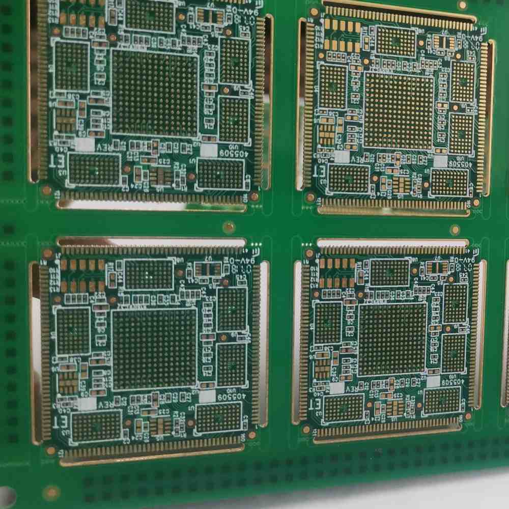
High density interconnect (HDI) is an advanced circuit interconnect technology that allows for higher wiring density and component placement compared to traditional printed circuit boards (PCBs). HDI has tightly spaced traces and microvias that connect multiple PCB layers allowing higher component density and more robust connections. This enables smaller, lighter, and higher performance electronic devices and products.
HDI technologies provide several key benefits:
- Smaller interconnect pitches down to 15-20μm
- Finer line and space geometries down to 10μm
- Higher wiring densities up to 1000 traces per inch
- More PCB layers connected with microvias
- Reduced weight and size of finished circuits
- Improved electrical performance and signal integrity
- Greater design flexibility
HDI has enabled shrinking of electronic devices and integrating more functionality and performance. It is widely used in consumer electronics, telecommunications, industrial, automotive, aerospace, and military applications.
HDI PCB Technology Overview
HDI utilizes several advanced PCB fabrication techniques:
Tightly Spaced Traces
HDI allows much finer traces with smaller widths and spacing between copper traces. This increases the routing density, allowing many more traces to fit in the same area.<div class=”table-wrap” markdown=”block”>
| PCB Type | Minimum Trace/Space |
|---|---|
| Standard PCB | Around 100μm |
| HDI PCB | 15-20μm |
</div>
The tighter trace geometries are achieved using laser direct imaging (LDI) which can pattern very fine lines.
Microvias
HDI employs microvias with diameters typically 50-100μm to interconnect between layers. The microvias are laser drilled with precise accuracy. This allows connections between layers spaced much closer together compared to through-hole vias in regular PCBs.<div class=”table-wrap” markdown=”block”>
| PCB Type | Minimum Via Diameter |
|---|---|
| Standard PCB | Around 200μm |
| HDI PCB | 50-100μm |
</div>
The small microvias facilitate densifying the vertical connections between layers in addition to the tight horizontal trace spacing.
More PCB Layers
HDI designs utilize more laminated PCB layer pairs, typically 6 to 12 layers. The additional layers connected by microvias provide more routing channels. Prepregs with very low dielectric thickness (~50μm) separate the layers.
Fine Line Patterning
Advanced lithographic patterning techniques like laser direct imaging (LDI) and photovia processes allow forming fine line circuits down to around 10μm width on HDI boards. This enables integrating components and connections at very high densities.
Sequential Buildup
HDI PCBs are fabricated using a sequential laminating process that embeds a core circuit in alternating layers of dielectric and copper. This allows “sandwiching” the fine line inner layers within the core and outer layers with lower density traces. The core provides mechanical support while the thin layers are for high density wiring.
Advanced Dielectrics
Low loss, high performance dielectric materials are required to maintain signal integrity in HDI boards. These include high glass transition temperature (Tg > 170°C) thermoset resins with low moisture absorption, low CTE, and smooth copper adhesion. Some common HDI dielectrics are polyimides, bismaleimides, hydrocarbon based materials, and liquid crystal polymers.
HDI Design and Fabrication Process
The design and fabrication process for HDI boards involves:
Layout
HDI layout employs CAD tools with advanced features for trace/space design rules, microvia design, and 3D modeling of the layer stackup. The designer places components and routes traces optimizing for high density and electrical performance.
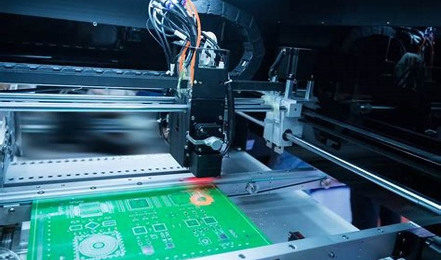
Imaging
A laser direct imaging (LDI) system patterns the fine line trace geometries and microvias. LDI provides high resolutions down to ~10μm and positional accuracy of under 5μm.
Layer Stackup
The HDI buildup process uses a thick core in the center, embedded trace layers, and alternating thin dielectrics and copper layers. This is repeated to construct anywhere between 6 to 12 layers.
Lamination
Thin dielectric films are laminated using advanced techniques to avoid trapping air and ensure dimensional stability. Temperature and pressure profiles are optimized to embed layers without deformation.
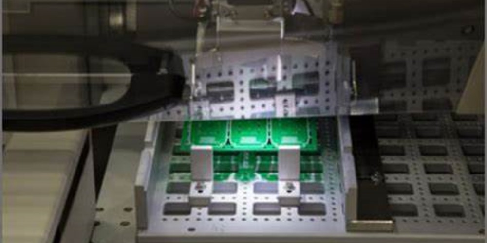
Microvia Formation
Microvias with 50-100μm diameters are laser drilled through multiple layers to form the vertical interconnects between trace layers.
Metallization
An electroless plating process uniformly deposits initial copper to coat all the microvia holes and surfaces. Electroplating then builds up the required copper thickness.
Outer Layer Processing
Conventional lithography, etching, stripping, and interconnect techniques are used for the lower density outer layers of the PCB.
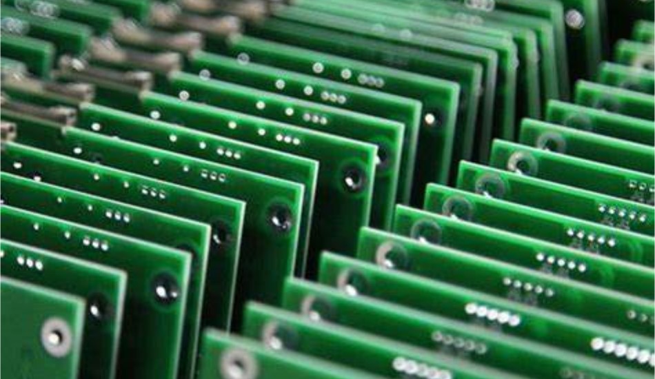
Final Finish
Finished boards undergo electrical testing, cleaning, surface treatments, solder mask application, protective coatings, legends, etc. prior to delivery.
HDI Materials and Fabrication Challenges
While HDI provides substantial benefits, the materials and processes pose challenges including:
- Achieving very fine geometries and small tolerances
- Eliminating defects and holes in thin laminate films
- High degree of accuracy in laser drilling microvias
- Potential thermal expansion issues with dissimilar metal and dielectric layers
- Maintaining dimensional stability of layers during lamination
- Plating very high aspect ratio microvias reliably
- Dealing with via-in-pad connections
- Restricted thermal management due to dense buildup
- Modeling signal and power integrity effects
- Mitigating moisture absorption in thin films
- Achieving high yields and reliability
These challenges make HDI PCBs more complex and expensive to fabricate compared to conventional PCBs. But the technical capabilities of HDI enable continuing miniaturization and performance advancements in electronics.
Applications of HDI
The small geometries, high wiring density, and interconnect capability of HDI make it an enabling technology for many advanced electronic products including:
Consumer Electronics
HDI is widely used to make the PCBs inside smartphones, tablets, laptops, wearables, game consoles, and other modern compact consumer electronics. The multilayer HDI boards integrate the dense component layouts in these devices.
Telecommunications
Networking hardware like routers and switches rely on HDI PCBs to provide high speed signal routing and reliable connections in complex multilayer designs.
Automotive Electronics
Automotive electronics are rapidly increasing in sophistication. HDI allows integrating many sensors, processors, and modules within the tight confines of a vehicle.
Medical Devices
Advanced medical electronic devices use HDI boards due to the ability to incorporate more functionality within smaller products like hearing aids and implantable devices.
Aerospace/Military
Size, weight, and electronics performance advantages make HDI suitable for space, avionics, radar, and other high reliability defense applications.
IoT Devices
For compact Internet of Things sensor nodes and hardware, HDI provides a means to achieving small form factors with wireless connectivity.
As electronics become smaller, more powerful, and feature-packed, HDI will continue growing in dominance for interconnect solutions. HDI performance now surpasses what regular PCBs can achieve.
Current and Future Outlook for HDI Technology
HDI has transitioned from a specialty PCB fabrication process to a mainstream interconnect solution that most electronics manufacturers now rely on for their designs. According to industry estimates, the HDI PCB market is forecast to grow from $9.8 billion in 2021 to around $27 billion by 2029 for a compound annual growth rate (CAGR) of 15%.
Several technology trends are driving increased adoption of HDI:
- Continued miniaturization of electronics
- Higher speeds and bandwidth demands
- Growth in advanced consumer tech like wearables and IoT
- Increasing electronics content in vehicles
- Rise of 5G networks and devices
On the technology horizon are advances like substrate-like PCBs incorporating HDI, conductive inks for fine printing of circuits, newer materials, and HDI designs with over 20 layers.
HDI technology will evolve to meet the roadmaps for increasing performance, functionality, and shrinking size of electronic products. HDI provides the sophisticated interconnect foundation for supporting all the advanced IC integration in modern electronics.
FAQs About High Density Interconnect PCBs
What is HDI in PCBs?
HDI or high density interconnect refers to an advanced set of PCB fabrication techniques that enable extremely fine traces, small microvias, and dense component layering. This allows much higher wiring densities and component packing compared to traditional PCBs.
What are the key features of HDI?
- Very fine trace widths and spaces down to 15-20 microns
- Microvias with diameters from 50 to 100 microns
- Multiple layers connected by high density microvias
- Up to 1000 traces per inch (TPI) routing density
- Overall enabling of smaller and higher performance PCBs
How is an HDI PCB constructed?
HDI uses a core circuit layer, embedded trace layers, and a sequential buildup process to construct up to 12 or more alternating thin dielectric and copper layers. The trace layers are connected by laser drilled microvias. Lamination, imaging, and plating steps bond the layers.
What are the main benefits of using HDI PCBs?
HDI provides:
- Smaller electronics due to higher component densities
- Lightweight and thinner circuit boards
- Improved electrical performance at high frequencies
- Multi-gigabit data rates within PCBs
- Miniaturization beyond limits of conventional PCBs
- Increased functionality and complexity of devices
What types of products typically use HDI PCBs?
HDI is the PCB technology of choice for building many modern compact and high performance electronics:
- Smartphones, tablets, laptops
- Networking hardware like routers
- Wearable technology
- Internet of Things (IoT) devices
- Advanced driver assistance automotive electronics
- Aerospace avionics systems
- Medical devices and instruments
What are some of the challenges with HDI fabrication?
HDI is more complex and costly to manufacture than standard PCBs. Key HDI fabrication challenges include:
- Achieving very tight tolerances on line dimensions and alignments
- Eliminating any defects in thin dielectric films
- Precisely laser drilling small diameter microvias
- Dealing with via-in-pad connections
- Maintaining dimensional stability during lamination
- Yield and reliability factors


Leave a Reply