Introduction
As electronic devices continue to get smaller and more complex, the printed circuit boards (PCBs) inside them must adapt. High-density interconnect (HDI) flex PCBs are an advanced PCB technology that allows for the miniaturization and improved performance required in today’s electronics.
HDI flex PCBs provide several advantages over traditional PCBs:
- Extremely fine traces and spaces
- More routing layers
- Blind and buried vias
- Flexible and rigid-flex constructions
- Advanced materials
This enables higher component density, smaller and thinner end products, improved high-speed performance, and more complex circuit designs. HDI flex PCBs are essential for the latest smartphones, wearable devices, medical devices, automotive electronics, and more.
What are HDI Flex PCBs?
HDI flex PCBs utilize advanced design and manufacturing processes to create boards with features much finer than standard PCBs. Some key characteristics include:
Fine Lines/Spaces
- Traces and spaces down to 15-20μm, versus 100-150μm on standard PCBs
- Allows placing components closer together
More Layers
- Up to 20-30 conductive layers, versus 2-8 on standard PCBs
- Provides more routing channels for complex circuits
Blind and Buried Vias
- Vias connect between inner layers only, without occupying outer layer space
- Allows higher component density
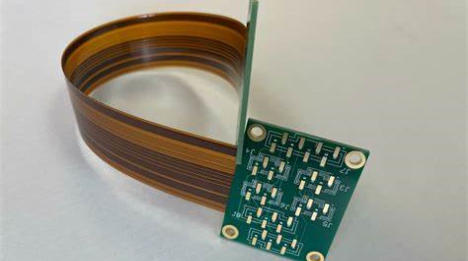
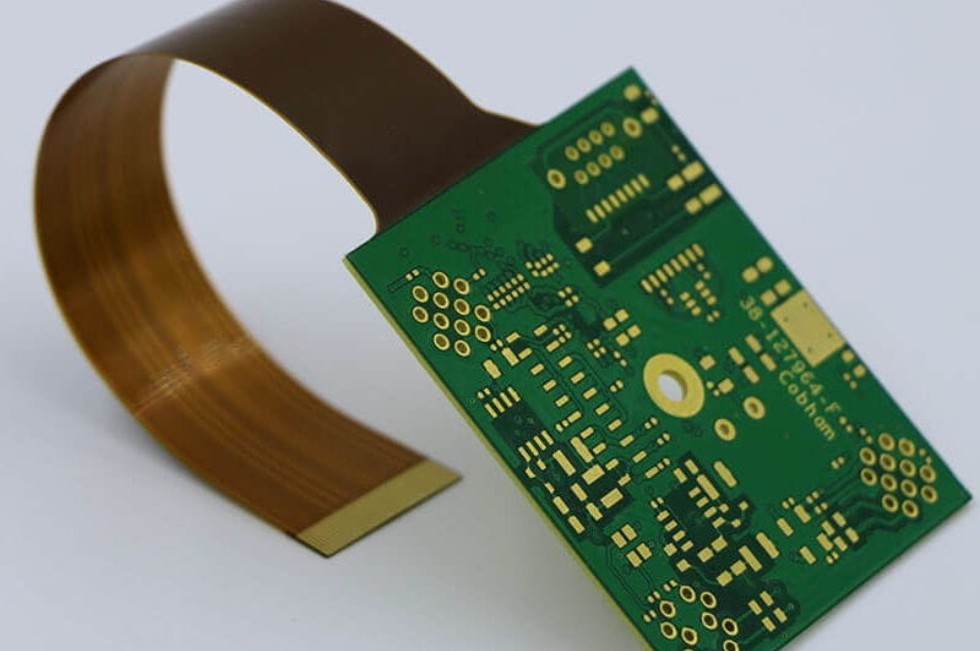
Flexible and Rigid-Flex Constructions
- Combines rigid PCB and flexible circuit technologies
- Enables bending and folding in end products
Advanced Materials
- Thin cores, high Tg resins, modified dielectrics
- Provides electrical and mechanical performance
Why Are HDI Flex PCBs Needed?
There are several main drivers behind the growing adoption of HDI flex PCB technology:
Miniaturization
As devices like smartphones, wearables, and medical devices shrink, the PCBs inside them must shrink as well. HDI flex allows fitting more circuitry into a small space.
Increased Functionality
With more components and features crammed into small products, PCBs require more routing layers and higher densities. HDI flex provides this.
High-Speed Signals
Faster processors, high-resolution displays, and other demands require handling high-speed signals across PCBs. HDI flex supports the tight impedance control needed.
Component Integration
Integrating components like processors, memories, and sensors into a single package is an ongoing trend. HDI flex can interconnect the dense interface arrays.
Flexibility/Bendability
Many applications from wearable gadgets to implantable medical devices require a degree of bendability. HDI flex PCBs provide this.
In summary, HDI flex PCB technology is nearly mandatory for product miniaturization, performance, and innovation in multiple industries.
HDI Flex PCB Materials & Construction
HDI flex PCBs utilize a number of advanced materials and design features to achieve their high performance and miniaturization.
Dielectric Materials
The insulating dielectric layers of HDI flex PCBs use materials engineered for tighter specifications and thinner constructions. Common materials include polyimide, liquid crystal polymer (LCP), and others. The dielectric constant and loss tangent are important electrical parameters.
Conductive Layers
Very thin copper foils, down to 1-2oz in weight, are used along with surface treatments to enable fine line patterning. The foil can be rolled or electrodeposited copper.
Vias
Laser-drilled microvias with diameters below 50μm help connect layers while occupying little space. As mentioned, blind and buried vias are heavily used.
Stiffeners
Since HDI flex PCBs have thin, flexible dielectrics, stiffeners made of materials like aluminum or FR4 may be added in certain areas to provide mechanical rigidity.
Coverlay
A solder mask coverlay can be laminated over the traces for protection, improved moisture resistance, and to facilitate soldering. Polyimide coverlay withstands flexing.
Pads/Land Patterns
To match component interconnects, small pad sizes and pitches under 100μm are standard. High-density interconnect (HDI) design rules are followed.
Plating
Traces are plated for conductance and solderability. Immersion silver, immersion gold, and electrolytic nickel/gold are common final platings.
HDI Flex PCB Fabrication Process Overview
Fabricating HDI flex PCBs requires specialized manufacturing capabilities beyond standard PCB production. Here is a simplified overview:
Imaging/Lithography
A liquid photoimageable dielectric (LDI) is laminated onto a base metal foil layer and imaged to define the fine traces, spaces, and vias. Laser direct imaging (LDI) is used.
Pattern Plating
Openings in the imaged dielectric are plated up to form the circuit traces and conductive thru-hole walls. Copper is typically plated.
Outer Layer Lamination
Additional dielectric and foil layers are bonded in a lamination press to build up the designed layer stackup. Alignment is critical.
Via Formation
Microvias are laser drilled through the dielectric to interconnect layers. Depth and taper must be tightly controlled.
Surface Finishes
Traces are plated with metallic finishes to protect against oxidation and provide solderability. Common finishes are ENIG, ENEPIG, Imm Ag, etc.
Singulation
The panelized boards are routed, punched or laser cut to separate into individual HDI flex PCBs. Automated optical inspection occurs.
This provides a simplified view of the complex process steps required to produce advanced HDI flex PCBs. Each step must be performed with extreme precision on industrial scale equipment.
HDI Flex PCB Design Guidelines
To successfully design an HDI flex PCB that can be manufactured requires adhering to constraints around trace/space, via sizes, and other parameters. Here are some key guidelines:
- Minimum trace/space: Follow manufacturer’s capabilities, typically 15-20μm range
- Minimum microvia diameter: 50μm or lower; laser drilled with tight registration
- Pad size/pitch: Scaled down vs standard PCBs, often less than 100μm pitch
- Layer stackup: Build with thin dielectrics around 0.5-3 mils thick per layer
- Impedance control: Matched lengths, minimized stubs, ground plane clearance
- Flex areas: Use polyimide dielectrics and coverlay, control bend radius
- Stiffeners: Incorporate metal or FR4 stiffeners for rigidity when needed
- Component selection: Choose appropriate small package components and interconnects
- HDI design rules: Account for vias/traces overlapping, acute angles, annular rings
Collaborating with the PCB manufacturer during design is highly recommended to ensure manufacturability and optimize the HDI flex PCB layout.
HDI Flex PCB Applications
The unique benefits of HDI flex PCBs make them an enabling technology across a diverse range of products and applications. Here are some examples:
Smartphones
HDI flex allows smartphones to pack more computing power and features into ever more compact mobile devices with sleek industrial designs. The PCBs interconnect high pin count processors, memories, wireless chips, sensors, and other components.
Wearable Electronics
For smartwatches, fitness trackers, VR headsets, and medical wearables that conform to the human body, HDI flex provides the ideal combination of small size, light weight, and bendability needed.
Internet of Things (IoT)
Interconnecting multiple sensors, processors, and wireless modules within the tiny footprints required by IoT edge nodes is made possible with HDI flex PCBs.
Automotive Electronics
The boom in cameras, radar, infotainment, and electronics for self-driving cars relies on HDI flex PCBs that can withstand vibration, heat, and space constraints.
Medical Devices
Implantable and wearable medical devices demand HDI flex PCBs that provide connectivity and high reliability within extremely compact form factors.
Aerospace/Defense
Mission-critical electronics for aerospace and defense need HDI flex PCBs that deliver fail-safe interconnects with redundancy and anti-tamper features within tight confines.
This is just a sampling of the many application spaces that can benefit from the unique capabilities of HDI flex PCB technology.
HDI Flex PCB Fabrication Technology Comparison
There are two main fabrication technologies used to produce HDI flex PCBs:
Modified Semi-Additive Process (mSAP)
This process creates the circuit traces by selectively plating copper into an imaged dielectric layer. It provides fine traces but limted alignment accuracy between layers.
Laser Direct Imaging (LDI)
With LDI, each dielectric layer is laminated, imaged, and pattern plated. Superior alignment and higher layer counts are achievable compared to mSAP.
Here is a comparison between mSAP and LDI:
| Parameter | mSAP | LDI |
|---|---|---|
| Minimum Trace/Space | 20/20 μm | 15/15 μm |
| Layer Alignment Accuracy | ~ 25 μm | < 5 μm |
| Max Routing Layers | 6-8 | 20-30+ |
| Flexible Dielectrics | Limited | Wide range |
| Via Types | Thru-hole | Blind/buried |
| Design Freedom | Restricted | Very High |
As the table illustrates, LDI provides finer features, superior alignment, more layers, and greater design freedom overall. The tradeoff is higher costs compared to mSAP.
HDI Flex PCB Cost Considerations
While HDI flex PCBs provide unparalleled interconnect density and performance, the advanced materials and fabrication processes involved do come at a cost premium versus standard PCBs. Here are some of the key factors:
- Tighter tolerances require higher precision equipment and lower yields
- Additional process steps like lamination and laser drilling
- Thinner dielectric materials are more expensive
- Each additional metal layer adds significant cost
- Advanced surface finishes have higher material expenses
- Lower volume production means less economy of scale
However, the value of the space savings, miniaturization, performance gains, consolidated components, and product features enabled by HDI flex PCB technology make the additional costs justifiable for many applications. And as volumes increase over time, costs can be expected to decrease as well.
Conclusion
HDI flex PCB fabrication represents a major technology evolution enabling the ongoing miniaturization and innovation in electronics. By bringing the capabilities of fine features, high layer counts, advanced materials, and flexible circuitry together, HDI flex PCBs will be a core platform for product development across industries for the foreseeable future. With careful design tailored to manufacturing capabilities, the benefits of this technology can be fully realized.
Frequently Asked Questions
What are some key differences between HDI flex PCBs and traditional rigid PCBs?
Some of the main differences are:
- Much finer trace widths/spacing (15-20um vs 100-150um)
- Ability to incorporate flexible circuits
- Far greater number of routing layers (20+ vs 2-8 typical)
- Extensive use of microvias, including blind/buried vias
- Thinner dielectric materials, allowing layer stackups under 1mm
- Significantly higher fabrication complexity and cost
What design software tools are typically used for HDI flex PCBs?
Most designers use mainstream PCB design packages like Altium, Cadence Allegro, and Mentor Xpedition. These tools allow setting up designs with HDI stackups, trace/space rules, microvia sizes, and export to manufacturing.
How are components attached to HDI flex PCBs?
Given the fine pitches involved, small surface mount packages like 0201 and 01005 metric are heavily used. Micro BGA bonding and high-precision flip chip attach are other common methods.
Does flexing the HDI board shorten its lifetime?
With proper design, material selection, and bend radius control, HDI flex PCBs can withstand thousands or tens of thousands of dynamic flex cycles before fatigue becomes a concern. The application determines requirements.
What types of testing are performed on HDI flex PCBs?
Testing includes electrical testing of shorts, opens, and impedance; Automated Optical Inspection (AOI); and environmental stress testing of bend cycles, vibration, thermal shock, and humidity as required by the application.


Leave a Reply