Introduction
Printed circuit boards (PCBs) are essential components in nearly all modern electronic devices. As electronics become smaller, faster and more complex, the circuit boards that connect and support these intricate systems must advance as well. High density interconnect (HDI) PCBs represent the cutting edge in printed circuit board design and fabrication. With their extremely fine lines, high component density, and complex layering, HDI boards enable the miniaturization and increased capability of today’s electronics. In this article, we’ll take an in-depth look at HDI technology and examine what sets these boards apart.
HDI Circuit Board Basics
HDI printed circuit boards contain very precisely etched, ultra-thin copper lines that enable connections to be packed more densely across the board. While conventional PCB trace and space widths range from 4-8 mils, HDI boards achieve trace widths down to 2 mils with 1 mil spacing between traces. This compact construction allows for more signal paths in a given area, permitting greater complexity and component integration.
In addition to finer trace dimensions, HDI boards utilize thinner dielectric material between copper layers, permitting more layers to fit in a given thickness. Where standard circuit boards often contain 4-8 conductive layers, HDI boards may incorporate 10 layers or more by stacking extremely thin insulating dielectric films. More available “real estate” equates to higher component density and more intricate circuit designs.
Key Characteristics of HDI Boards:
- Trace/space dimensions under 4 mils (down to 2/1 mil)
- Dielectric layer thickness under 3 mils
- High layer count – 10+ layers possible
- Laser drilled microvias under 8 mils for interlayer connections
- Fine line discrete and integrated components
- Extremely high wiring densities (>1000 nets/in2)
This combination of fine features enables an HDI board to incorporate greater functionality into a small footprint, a major advantage for densely packed mobile consumer electronics and telecommunications devices.
HDI PCB Fabrication Process
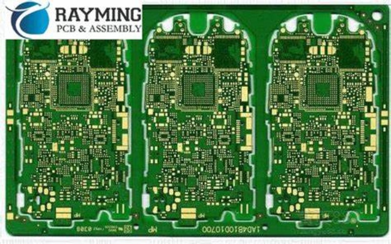
Constructing HDI circuit boards requires specialized fabrication techniques to achieve the trace dimensions, layer registration, and interconnections necessary. Here are some of the key steps:
Fine Line Patterning
The first necessity in HDI fabrication is generating extremely fine copper traces and spaces down to 2 mils wide. To accomplish this, most HDI boards use a photolithographic process with a laser direct imaging (LDI) system. This technique can precisely image and etch the necessary trace widths and spacing onto thin copper foils.
Thin Dielectric Layers
Polyimide films as thin as 1 mil are layered between the etched copper foil circuitry, allowing high layer counts in minimal thickness. The layers are precisely aligned using registration holes or fiducials to provide vertical connections between layers.
Microvias
Small vias generated by an excimer laser drill provide vertical interconnections between the thin layers. These microvias measure 6 mils in diameter or less. The walls are plated to form conductive connections between layers separated by the thin dielectric films.
Discrete Component Attachment
Tiny discrete components including resistors, capacitors, and diodes are soldered directly onto the surface of HDI boards to maximize space efficiency. These 0201 or 01005 chip components are just 0.4mm to 0.6mm in size.
IC Attachment
Bare die or flip chip mounting attaches unpackaged integrated circuits directly to the HDI board surface. This provides ultimate space utilization. Wire bonding or thin solder bumps connect IC input/output pads to board traces.
Final Assembly
HDI boards are finished by applying solder mask, silkscreen legends, and surface finishes as required. Rigorous electrical testing verifies board function prior to shipment and installation. Careful handling procedures protect the fragile traces and components.
Proper design rules, fabrication processes, and assembly methods are critical to producing fully functional high density interconnect circuit boards. When executed correctly, HDI provides the highest wiring densities of any PCB technology available today.
Comparison of HDI Boards vs Standard PCBs
| Parameter | Standard PCB | HDI PCB |
|---|---|---|
| Trace Width/Spacing | 4-8 mil | 2-3 mil |
| Dielectric Thickness | 2-5 mil | 0.5-3 mil |
| Via Size | 8-12 mil | 4-6 mil |
| Layers | 4-16 | 10-20+ |
| Line Density | 500-800 in2 | 1000+ in2 |
Applications of HDI Technology
The unique properties of HDI printed circuit boards lend themselves to applications where high component density, complex circuit routing, and miniaturization are required. Here are some of the leading applications taking advantage of HDI PCB technology:
1. Smartphones
Smartphones pack tremendous processing power and features into a pocketable form factor. HDI allows smartphone PCBs to accommodate more memory, beefier processors, wireless radios, and additional components by increasing wiring density and trace routing channels.
2. Wearable Devices
Wearable products like smart watches rely on HDI to build full functionality into extremely compact assemblies. The boards provide interconnectivity for displays, sensors, batteries, and processors within limited space.
3. Internet of Things (IoT)
Network-connected devices from home appliances to medical equipment to automotive systems often leverage HDI circuit boards. The technology permits complex networking hardware and antennas to fit into the constrained IoT product enclosures.
4. High Speed Communications
HDI provides closely matched trace impedances for routing high frequency signals up to microwave bandwidths. This makes the boards ideal for radio frequency (RF) and millimeter wave applications.
5. High Pin Count ICs
Processors and application specific integrated circuits (ASICs) with over 1,000 input/output contacts can be accommodated on HDI boards, where fine lines and spaces connect tightly packed component lead pads.
6. Portable Electronics
Mobile consumer electronics like tablets and laptops depend on HDI PCBs to achieve ever improving performance and features while reducing size and weight. The boards integrate processors, memory, sensors, and peripherals.
7. Medical Electronics
Advanced medical devices for imaging, diagnostics, therapy, and implanted applications utilize HDI boards to package necessary electronic functionality into housings that meet demanding size constraints.
8. Automotive Electronics
Automotive cameras, radar modules, control units, and infotainment systems need HDI circuit boards to condense electronics into available dash and cabin space as features grow.
9. Aerospace and Defense
Avionics, guidance systems, and munitions require rugged, high density electronics. HDI provides solutions where size, weight, and reliability are critical in extreme environments.
As electronic devices and components continue trending toward smaller scales and greater sophistication, HDI PCB fabrication and assembly will remain an enabling technology across nearly every industry.
HDI Design Considerations
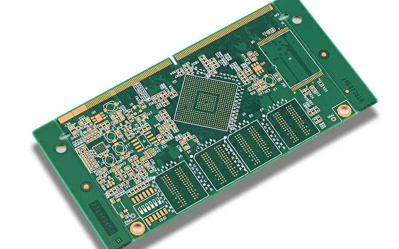
Designing a high density interconnect printed circuit board requires special considerations to leverage the benefits while avoiding pitfalls. Here are some key HDI design guidelines:
- Work closely with your board fabricator – Their capabilities will dictate trace width, layer count, and via feasibility based on equipment.
- Follow fabrication design rules – This ensures your layout adheres to the PCB manufacturer’s processing limitations.
- Use gridded routing – Even trace widths and spacing will prevent electrical issues and fabrication problems.
- Include impedance controls – Match trace geometry to required impedance for high speed signals.
- Incorporate plane layers – Solid power and ground layers provide stability, shielding, and heat dissipation.
- Allow for via capture pads – Vias need adequate annular rings and landing areas on each layer for reliability.
- Watch out for stubs – Avoid stubs and tuning circuits that may resonance at high frequencies.
- Include test points – Provide adequate test points for fabrication and assembly verification.
- Plan for flatness – Thin, high layer count designs can warp. Use symmetry and consider stiffeners.
- Control coefficients of thermal expansion (CTE) – Manage CTE mismatches to prevent stress on components.
- Validate assembly processes – Ensure your pick and place and soldering processes can handle ultra-fine component packages.
With careful HDI circuit board design catered to your product’s unique size, performance, and cost requirements, you can take full advantage of this powerful PCB technology.
The Future of HDI Technology
HDI circuit boards have progressed tremendously over the past decades in terms of achievable line width, layer count, and component densities. And development continues driven by the unrelenting pace of electronics innovation. Here are some directions HDI fabrication is headed:
- Even finer trace geometries below 1 mil to increase wiring density.
- New laser direct imaging systems to pattern ultra-fine traces.
- Thinner dielectric films below 1 mil to enable higher layer counts.
- Buried and blind microvias under 5 mils in diameter.
- PCBs integrating embedded active and passive components.
- Thermally conductive dielectric materials to dissipate heat efficiently.
- Improved registration accuracy for layer-to-layer alignment.
- Advanced reliability testing for material sets and process flows.
- Environmentally friendly manufacturing processes.
- Continued cost reduction through higher fabrication productivity.
Many industry experts foresee lines and spaces dropping below 1 mil in mainstream HDI technology within this decade. This will support chips with over 40,000 I/O pins in advanced smartphones, enable augmented reality glasses and heads up displays for vehicles, and facilitate extremely compact IoT sensors. The integration of active components into HDI boards themselves may also become practical in the coming years.
Conclusion
High density interconnect PCB technology enables the ongoing revolution in electronics toward ever smaller, faster, smarter, and more connected devices. With its ultrathin dielectric films, microscopic trace widths approaching 1 mil, and high layer counts, HDI provides a pathway to pack more functionality into less space. As electronics engineers continue to push the boundaries of what’s possible, innovative HDI circuit board fabrication and assembly will remain instrumental in turning designs into reality.
HDI PCBs – Frequently Asked Questions
1. How small can lines and spaces be fabricated on HDI boards?
Current mainstream HDI fabrication can achieve 2 mil lines and spaces. With advanced processes, trace widths down below 1 mil are possible for leading edge designs. The lower limit continues to be pushed down as laser direct imaging technology improves.
2. What are typical layer counts for HDI printed circuit boards?
Most HDI designs utilize 10 to 16 conductive layers. However, some designs employ 20 layers or more. The very thin dielectric films enable high layer counts in a reasonable board thickness.
3. How are layers aligned on HDI boards?
Precision registration and imaging systems align subsequent layers to within 1 micron accuracy. Registration holes, fiducials, and image recognition help optimize layer-to-layer alignment.
4. Can components be embedded within HDI boards?
Some fabrication processes permit active and passive components to be embedded within the HDI board layers. This provides ultimate space utilization. However, the approach also increases cost and complexity significantly.
5. What are the tradeoffs between HDI vs standard PCBs?
HDI provides the highest wiring density but also comes with higher cost. Standard PCBs offer lower cost, less complexity, and wider fabrication capability at the expense of density. The optimal choice depends on the design requirements.
Leave a Reply