
Introduction
Printed circuit boards (PCBs) are an essential component of most modern electronic devices. From smartphones and computers to industrial equipment and medical devices, PCBs provide the foundation on which components are mounted and connected. As electronic devices have become more complex and packed with features, the demands on PCBs have increased dramatically. This is where high-density interconnect (HDI) PCBs come into play.
HDI PCBs provide higher wiring densities than conventional PCBs, allowing more connections and components to be packed into a smaller space. This article will examine what makes HDI PCBs different, why they are important for modern electronics, and some of the key benefits they provide.
What Are HDI Printed Circuit Boards?
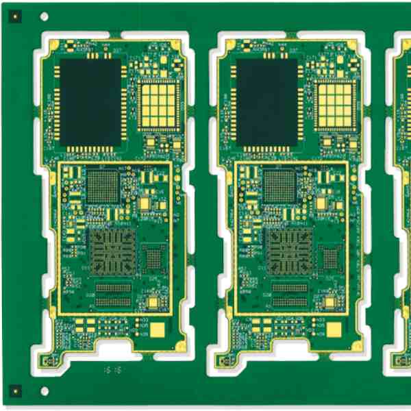
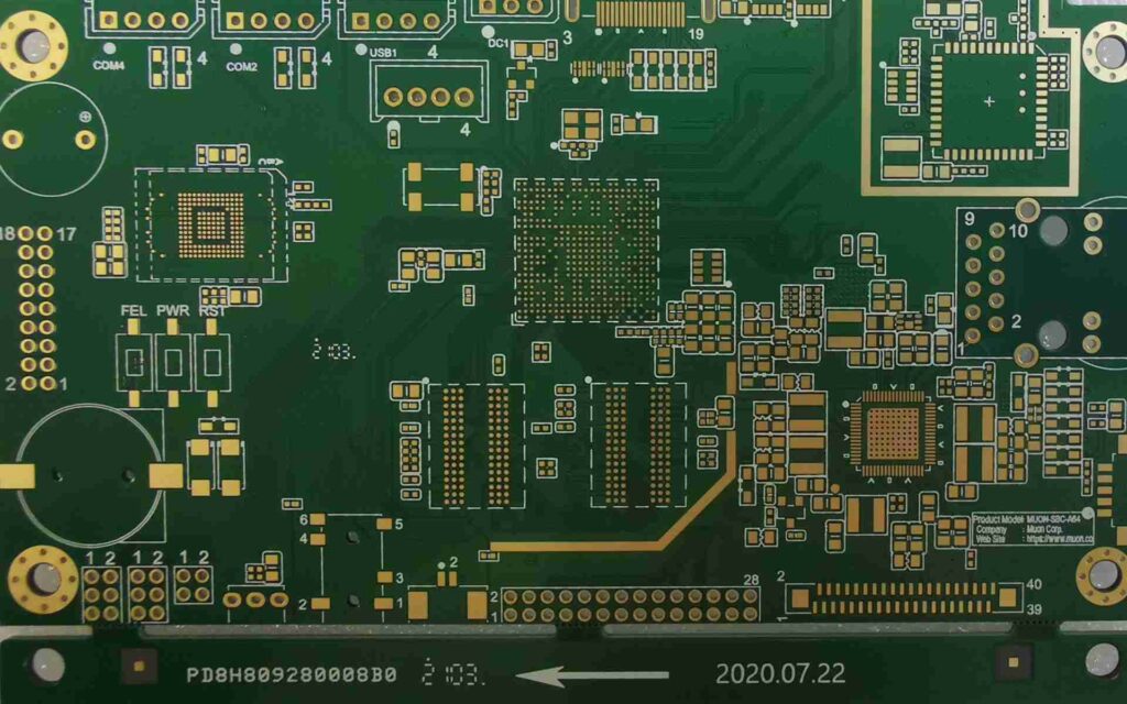
HDI PCBs use densely packed microvias and thin circuitry to achieve high interconnect densities not possible with standard PCB manufacturing processes. Some key characteristics of HDI PCBs include:
Small Vias and Trace Widths
- Microvias with diameters less than 150 microns, compared to typical via diameters of 250-400 microns.
- Fine line traces and spaces less than 100 microns. Standard PCB trace widths are around 200 microns.
More Routing Layers
- HDI PCBs typically have 6-12 conductive routing layers compared to 2-6 layers in conventional PCBs.
Thinner Dielectric Material
- Dielectric layers as thin as 25-50 microns vs. typical 100 micron dielectrics. Thinner dielectrics allow tighter spacing between circuit layers.
Laser Drilled Microvias
- Microvias are drilled with laser technology for precision accuracy. This allows high densities with reliable interlayer connections.
Sequential Buildup Process
- Circuitry is built on the board layer-by-layer rather than all at once like standard PCBs. This enables formation of complex HDI stackups.
These features allow HDI PCBs to have 5-10 times greater interconnect density than standard PCBs.
Table Comparing HDI and Standard PCB Characteristics
| Parameter | Standard PCB | HDI PCB |
|---|---|---|
| Via Diameter | 250-400 microns | Less than 150 microns |
| Trace/Space Width | 200 microns | Less than 100 microns |
| Routing Layers | 2-6 | 6-12 |
| Dielectric Thickness | 100 microns | 25-50 microns |
| Drilled Vias | Mechanical | Laser |
| Build Process | Single Stage | Sequential |
Why Are HDI PCBs Important?
The dense integration of microprocessors, memory, and other components on circuit boards requires interconnect technologies that can accommodate the high IO densities. HDI PCBs fulfill this role in many advanced electronics.
Miniaturization
HDI PCBs are essential for product miniaturization. By packing more functionality into a smaller PCB area, HDI technology enables smaller and thinner end products. A smartphone PCB built with HDI methods can be over 50% smaller than an equivalent standard PCB.
High-Speed Circuits
The short trace lengths, tightly matched lengths, and electromagnetic isolation of microvias in HDI PCBs are ideal for high-frequency analog and digital circuits. HDI boards support data rates over 1 Gbps for advanced communications and computing applications.
Cost Reduction
By enabling miniaturization and integration of components in a smaller PCB footprint, HDI technology reduces the overall electronics packaging cost. The boards themselves are more expensive to fabricate, but the total system cost savings more than compensates for the HDI PCB premium.
Reliability
Despite their density, HDI PCBs can offer higher reliability than standard boards. The fine geometries and buildup process result in lower stress and better connectivity in HDI stackups. Microvias have 5-10 times the connection strength of plated through holes.
Key Benefits of Using HDI for PCBs
Let’s examine some of the major benefits designers can realize by utilizing HDI printed circuit boards:
1. Design Flexibility
With HDI manufacturing, designers have unprecedented freedom in laying out board circuitry. More routing layers and the ability to place microvias right where needed provides tremendous flexibility. Spacing constraints are greatly reduced. Critical signals can be isolated on inner layers. And length matching for high-speed signals is facilitated.
2. Increased Component Density
The high interconnect density of HDI PCBs allows fitting more components in a given area. This facilitates miniaturization, integration of functions, and embedding components like capacitors and resistors within the board itself. The result is higher functional density and often a reduced number of layers versus conventional PCB stackups.
3. Better Signal Integrity
Signal integrity is improved with HDI PCBs in multiple ways. The smaller vias allow shorter routing with less discontinuity. Ground planes can be placed closer to signals. Controlled impedance traces are easier with thinner dielectrics. Stubs and unwanted capacitance are reduced with fewer through holes. Together these factors improve signal quality at high frequencies.
4. Lower EMI and Crosstalk
Electromagnetic interference (EMI) and crosstalk between circuits are major concerns in dense, high-speed PCBs. HDI designs help mitigate these issues in several ways. First, signals operate at lower voltages due to tighter spacing. Second, there is increased isolation between layers with more ground planes and thinner dielectrics. And third, microvias allow detouring sensitive traces away from aggressor signals.
5. Multi-Gigabit Data Rates
The fine geometries, controlled impedances, and signal integrity of HDI PCBs support data rates up to 25 Gbps on copper traces. This enables high-speed communication links between ICs and data transmission rates fast enough for 100G Ethernet switches or 400G fiber optic gear. HDI provides the interconnection technology for terabit backplanes.
6. Improved Thermal Performance
HDI printed circuit boards often have better thermal characteristics than conventional PCBs in spite of their dense component packing. The additional inner layers provide more thermal conduction for heat spreading. And the reduced current loops lower resistive losses that contribute to heating. Improved thermal performance leads to better system reliability.
Applications Using HDI Technology
HDI PCBs now appear in a myriad of advanced electronic products where density, speed, and precision are important. Some examples include:
- Smartphones – HDI is essential for integrating high pin-count processors, memory, and other ICs into the compact smartphone form factor. Apple’s iPhone PCB is a well-known example of HDI.
- Wearables – Miniaturization needs make HDI a fit for smart watches, fitness bands, VR headsets, and medical wearables where space is extremely limited.
- Automotive – Driver assistance systems, infotainment units, and vehicle control systems rely on HDI boards for their complex circuitry.
- Medical – Implants, CT scanners, lab instruments, and other medical gear requires HDI’s dense, high-speed, and low EMI characteristics.
- Aerospace/Defense – Rugged electronics for guidance systems, communications, imaging, and avionics leverage HDI PCBs.
- High-End Computing – Supercomputers and data center servers depend on HDI technology for terabit backplanes and switch fabric.
So while hidden from view, HDI printed circuit boards play an important role across many advanced electronics sectors where performance and precision matter. As electronic systems continue to advance, HDI PCBs will take on even greater importance.
HDI PCB Design and Fabrication Considerations
Designing and manufacturing high-density interconnect PCBs requires special considerations and expertise. Here are some key points for engineers working with HDI technology:
- Simulation – The signal and power integrity needs of HDI designs makes simulation essential. Modeling tools like Ansys SIwave are used to optimize stackups.
- Fab Partner – Work with a PCB fabricator experienced in HDI processes. They can assist with DFM and provide technology options like microvias and fine line tolerances.
- Stackup – Pay special attention to layer stackup, sequencing, and lamination. This is crucial for reliable interconnections and preventing hot spots.
- Testing – HDI boards often require AOI, x-ray, and impedance testing to verify quality and reliability due to their tighter geometries.
- Rework – Repairs are difficult on dense HDI boards. Design with debug and rework capabilities in mind. Consider limitations on via plugging.
- Cost – While reducing system cost, HDI PCBs themselves cost more to fabricate. Weigh tradeoffs of HDI versus conventional boards or advanced packaging.
- DFM – Partner with your PCB supplier early to ensure manufacturability and yield. HDI processes have tighter margins and demand rigorous DFM.
Conclusion
High-density interconnect PCB technology enables the sophisticated and compact electronics permeating products we use everyday. Continued innovation in HDI will be crucial as electronic devices get smaller, faster, and more feature-rich. HDI allows PCBs to stay on pace with other advances in semiconductors, software, displays, and other technologies. With diligent design and fabrication, engineers can leverage HDI printed circuit boards to develop exceptional products.
Frequently Asked Questions
What are some key differences between HDI and conventional PCBs?
Some major differences are:
- Smaller microvias vs. standard drilled vias
- Finer trace geometries and spacing
- More routing layers, typically 8-10
- Thinner dielectric materials between layers
- Higher wiring densities and interconnectivity
- Laser drilled microvias for precision
- Sequential buildup process
Why does HDI enable higher component density on PCBs?
With the finer lines and spaces, microvias, and additional routing layers, HDI PCBs have 5-10X the interconnect density of regular PCBs. This allows placing more ICs and other components in a given board area by utilizing the extra interconnect capability.
What are limitations of HDI PCB technology?
Some limitations include:
- More difficult design and simulation
- Tighter fabrication tolerances
- Susceptibility to fabrication defects
- Advanced testing required
- Difficult rework and repair
- Higher fabrication costs
What types of products benefit most from using HDI PCBs?
Products where small size, high speed, and reliability are critical get the most advantage from HDI technology. This includes consumer devices like smartphones and wearables as well as high-end computing and medical equipment.
How are microvias used in HDI PCBs superior to plated through holes?
Microvias have much higher connection strength and conductivity than PTHs. There is also less capacitance since stubs are shorter. And spacing can be tighter due to the small via diameters. Microvias are also placed precisely only where needed.


Leave a Reply