Introduction
Printed circuit boards (PCBs) are essential components in nearly every modern electronic device, from smartphones and laptops to industrial equipment. Designing and manufacturing high-quality PCBs requires generating Gerber files, a standard file format used by PCB fabrication shops. This article will walk through the entire process of going from Gerber files to finished PCBs, covering key topics like:
- What are Gerber files and why are they important?
- Generating Gerber files from PCB design software
- Understanding the different types of Gerber files
- Preparing Gerber files for manufacturing
- Selecting a PCB fabrication shop
- Placing a PCB manufacturing order
- Receiving and inspecting finished PCBs
Follow these steps to smoothly convert your circuit designs into physical PCBs ready for electronics assembly.
What Are Gerber Files?
Gerber files are a standard file format used to convey PCB design data to manufacturing. They contain vector images describing the copper layers, silkscreen layers, solder mask layers, drill files, and other key aspects of the PCB. Gerber files are generated from PCB design software after the engineer has completed the circuit schematics and board layout.
Some key facts about Gerber files:
- Developed by Gerber Systems decades ago, hence the name
- 2D vector images, no 3D data
- ASCII text coordinates to describe primitives like lines/arcs
- Each layer of the PCB design has a separate Gerber file
- Used by virtually all PCB manufacturers
Because Gerber files contain the complete board fabrication data in a standard format, they allow PCB designers to send their files to any manufacturer worldwide. This gives great flexibility when sourcing PCB assembly services.
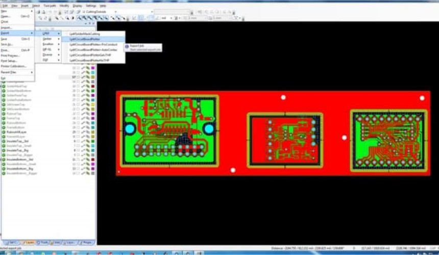
Generating Gerber Files
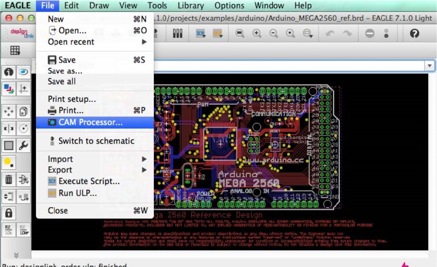
While the exact steps vary by CAD software, generating Gerber files typically involves:
- Completing all board layout and design rule checks
- Setting output options to generate Gerber/drill files
- Choosing file naming conventions
- Selecting options like coordinate format
Popular PCB design tools like Altium, Eagle, KiCad, OrCAD, and others have documentation detailing how to produce Gerber files. The settings may generate separate Gerber files for copper layers, silkscreen, solder mask, drill data, scoring lines, and other fabrication data required by the PCB manufacturer.
Here is an example workflow in Altium to generate Gerber files:
- Open the PCB design and run the Design > Validate Changes > Check PCB dialog to verify no errors
- Open the File > Fabrication Outputs dialog
- Select the Output Job File option and set the filename
- Adjust the Camtastic! settings as needed under Options > Camtastic! options
- Click OK to generate the Gerber files!
The result is a set of Gerber files ready for manufacturing. Now let’s look at the different types of Gerber files.
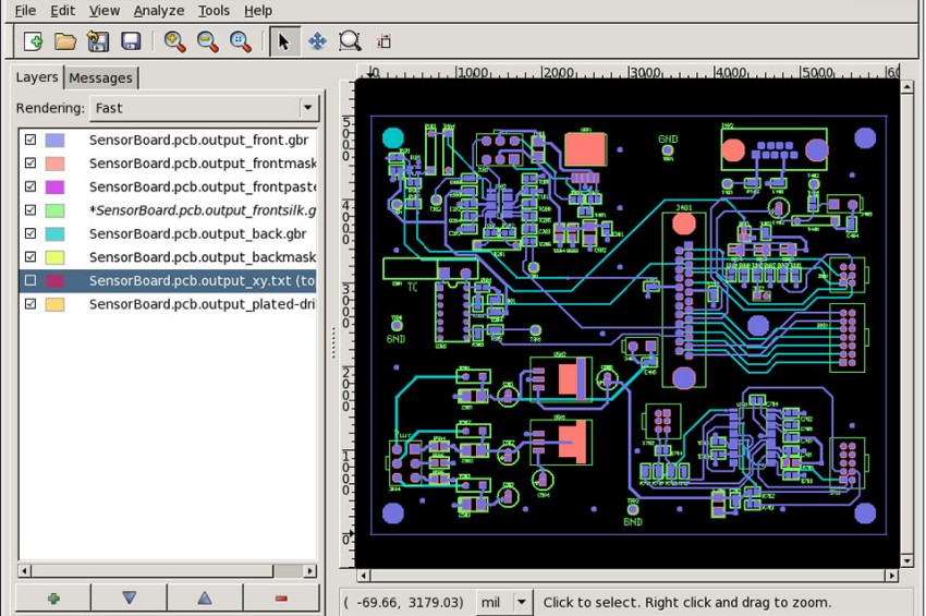
Types of Gerber Files
While there are many possible Gerber file layers, here are some of the most common:
| File Type | Description |
|---|---|
| Copper Layers | Describe the conductive copper traces on each layer |
| Solder Mask Layers | Define areas for solder mask application |
| Silkscreen Layers | Include graphics and markings printed on the PCB |
| Drill Drawing | Specifies hole sizes and locations |
| Board Outline | Outline of the board dimensions |
Here are some examples from a simple PCB design:
Top Copper Layer
Bottom Copper Layer
Top Solder Mask Layer
Top Silkscreen Layer
Drill Drawing Layer
Board Outline Layer
These are the primary layers needed to fabricate a finished PCB. Other special layers may be used in some cases.
Now let’s look at how to prepare these Gerber files for sending to a PCB manufacturer.
Preparing Gerber Files for Manufacturing
Before submitting Gerber files for PCB fabrication, it’s important to follow guidelines to ensure manufacturing success:
Include All Required Layers – Verify there is a Gerber file for every necessary fabrication layer. Omitted layers can prevent board fabrication.
Confirm Image Polarity – Make sure dark and clear areas of Gerbers correspond to conductive and non-conductive regions correctly.
Check Design Rules – Ensure board spacing and sizes comply with manufacturing capabilities, like minimum trace width, hole size, and spacing between copper regions.
Name Files Consistently – Use a consistent naming scheme for Gerber files so they can be identified easily.
Convert to Latest Gerber Format – Some PCB shops recommend converting files to the RS-274X format for best results.
Zip Files Together – Compress Gerber files into a single .zip archive to simplify transferring them to the PCB manufacturer.
Include Documentation – Provide any special instructions, board stackup diagrams, and documentation needed to understand the board fabrication requirements.
Following these tips will minimize delays and confusion during the PCB fabrication process.
Choosing a PCB Manufacturer
With the Gerber files prepared, the next step is selecting a PCB fabrication shop. Here are key factors to consider:
- Capabilities – Confirm the manufacturer can handle your board’s size, layer count, materials, tolerances, and electrical requirements.
- Quality – Look for manufacturers that follow rigorous quality control processes with high first-pass yield. Ask for example boards.
- Cost – Weigh costs across assembly services, production volumes, materials, and lead times. Get multiple quotes.
- Lead Time – Evaluate production lead times to meet your project timeline. Rush orders can increase costs.
- Location – Shipping costs and delays may be reduced by using local manufacturers. However, global sourcing provides flexibility.
- Reviews – Check customer reviews to evaluate manufacturers’ communication, customer service, quality consistency and overall reputation.
By comparing multiple PCB manufacturers using these criteria, designers can select the best production partner for their circuit board needs.
Placing a PCB Manufacturing Order
Once the PCB manufacturer has been selected, it’s time to setup the order. Here is a typical process:
- Upload Gerber files and documentation through the manufacturer’s website
- Select the required production specifications:
- Quantities
- Dimensions
- Materials like FR4
- Layer count
- Solder mask type
- Surface finish
- Silkscreen color
- Any other requirements
- Choose any additional services like assembly, testing, stencils, or special handling
- Accept the final quotation after all details are correct
- Make payment for engineering and production costs
- Receive order confirmation with estimated lead time
At this point, fabrication will begin based on the information provided. Be sure to carefully check that all production details match your PCB requirements before confirming the order. Contact the manufacturer immediately if any changes are needed to prevent production errors.
Receiving and Inspecting PCBs
Once the production lead time elapses, the PCB manufacturer will ship the finished boards. The typical process when receiving boards is:
- Inspect shipping boxes for damage indicating potential PCB damage
- Verify the quantities and board types match what was ordered
- Visually inspect one or more PCBs under light for physical defects
- Look for scratches, nicks, uneven solder mask, missing copper, out of tolerance spacing, etc.
- Check component holes and vias under magnification to confirm proper drilling
- If desired, run an electrical continuity test on nets to detect opens/shorts
- Carefully repackage boards if returning to manufacturer for rework
- Send prompt payment upon successful board receipt
- Provide feedback to the manufacturer on quality and experience
While the inspection process depends on the specific PCB, following these industry best practices helps identify any production issues early. This minimizes costs of defect discovery during subsequent assembly and testing.
Conclusion
This guide covered the end-to-end process of converting Gerber files into finished PCBs using professional board houses. By understanding these steps for generating, preparing, and inspecting Gerber files, electrical engineers can smoothly transform circuit designs into prototypes or production boards. Choosing the right PCB manufacturer and communicating effectively is also key to success. Following this checklist will produce high-quality PCBs tailored for electronics projects and products.
Frequently Asked Questions
What are some common problems when ordering PCBs?
Some common issues that can delay PCB orders include:
- Uploading incorrect or incomplete Gerber files
- Specifying board stackup, layer count, or materials incorrectly
- Having design rule errors like insufficient spacing
- Using incorrect footprint libraries resulting in wrong hole sizes
- Providing inadequate documentation of the board requirements
- Not confirming order details carefully before submission
- Not inspecting boards promptly upon receipt
How are surface finishes like ENIG and Immersion Gold different?
The PCB surface finish affects solderability, corrosion resistance, and long-term reliability. Common finishes include:
- ENIG (Electroless Nickel Immersion Gold) – Provides excellent solderability but higher cost
- Immersion silver – Lower cost but more prone to oxidation/tarnishing
- Immersion tin – Budget option but can create brittle intermetallics
- Hard gold plating – Very thick gold for harsh environments
What are panelization and breakout boards?
Panelization refers to manufacturing many smaller PCBs together on a larger panel that is later broken apart. This is done to reduce handling costs of small boards. Breakout boards temporarily connect panels for easier soldering and testing before individual boards are snapped apart.
Should PCBs be washed after fabrication?
Post-etch washing is often recommended to remove residual chemicals from fabrication. Washing helps prevent corrosion and enhances solderability. Typical wash processes use deionized water followed by baking boards dry.
How are multilayer PCB stackups designed?
Multilayer PCBs sandwich alternating layers of copper and dielectric material in a sandwich structure. Ground and power supply layers are typically on inner layers while signal routing is on outer layers. The order and thickness of each material must be defined in the stackup documentation.


Leave a Reply