Introduction to Gerber Files
Gerber files are the standard format used by PCB manufacturers for circuit board fabrication data. Gerber files contain 2D vector images describing the copper layers, solder mask, silkscreen, drill holes, and other aspects of a printed circuit board (PCB) design. The Gerber format was developed by Gerber Systems Corporation in the 1980s and has become the de facto standard for PCB layout data transfer.
Understanding Gerber files is crucial for electronics engineers and designers working on circuit board projects. This guide will provide an overview of Gerber file formats, how to generate Gerber files from EDA tools, best practices for file setup, and how to review Gerber data to ensure proper PCB manufacturing.
Gerber File Format Types
There are several different types of Gerber files, each containing data for a specific layer or attribute of the board. Here are the most common Gerber file formats:
Copper Layers
- Gerber RS-274X (.gbr) – The copper layers, including the top copper, bottom copper, and any internal copper layers.
- Gerber RS-274D (.gbd) – An older version of the copper layer format with limited image resolution.
Solder Layers
- Solder Mask (.gbs) – The solder mask layer which defines the solderable areas.
- Solder Paste (.gbp) – The solder paste layer which outlines where paste should be applied.
Silkscreen and Drill Files
- Silkscreen (.gbo) – The component legends and identifiers printed on the PCB.
- Drill (.drl or .ncb) – The location of drill holes and tool sizes.
- Profile (.gbr) – The board profile or outline.
Generating Gerber Files
Gerber files are generated from PCB layout software such as Altium, Eagle, KiCad, OrCAD, and others. The process involves going through an output procedure known as “CAM” (computer-aided manufacturing).
The CAM settings will determine which layers and features get output to Gerber files. It is critical to ensure the correct fabrication data is generated.
Here is a typical CAM output:
- Top Copper (.GTL)
- Bottom Copper (.GBL)
- Internal Layers (.G1, G2, etc)
- Top Solder Mask (.GTS)
- Bottom Solder Mask (.GBS)
- Top Silkscreen (.GTO)
- Bottom Silkscreen (.GBO)
- Drill file (.DRL)
- Board Profile (.GM1)
Best Practices for Gerber Setup

Follow these guidelines when generating Gerber files for PCB production:
- Include All Required Layers – Don’t forget vital fabrication data like the board outline layer.
- No Free Copper Pours – All copper pours should be covered by mask to avoid short circuits.
- Unique File Names – Name the files logically for easy identification (e.g. TopCopper.gbr)
- Keep File Extensions – Don’t change the .gbr, .drl extensions of standard layers.
- Metric Units – Set fabrication dimensions to millimeters (mm).
- Absolute Coordinates – Files should use absolute distance metrics, not incremental.
- Keep It Simple – Don’t include extra text, logos, or dimensions in files.
- Minimum Feature Sizes – Respect the manufacturer’s capabilities for trace width, spacing, etc.
- Include Netlist – Supply a netlist file for verification of layers.
- Zip Archive – Compress the Gerber folder to reduce file sizes.
Reviewing Gerbers Before Manufacturing
Before sending Gerber files off for PCB production, thoroughly inspect the layers to catch any potential errors:
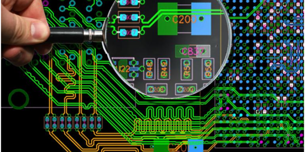
- Visual Review – Do copper traces and pads match the schematic? Is the silkscreen and solder mask correct?
- Dimensional Check – Verify board shape and footprint sizes are as expected.
- Cross-Probe – Load the Gerber into the PCB layout tool and cross-check layers.
- Design Rule Check – Use automated DRC tools to catch any clearance violations.
- Gerber Viewer – Use a viewer like GC-Prevue to thoroughly inspect all layers.
Taking the time to audit Gerber files is essential to avoiding costly manufacturing re-spins and production delays.
Gerber File Viewers
Specialized Gerber file viewers allow inspection of the individual PCB layers for errors:
| Viewer | Description |
|---|---|
| GC-Prevue | Advanced Gerber and drill file viewer |
| Gerbv | Open source Gerber viewer |
| ViewMate | Gerber viewer with measurement tools |
| Kicad StepUp | Built-in Gerber viewer in KiCad |
| IPE | Opens Gerber files along with other file types |
These viewers allow toggling on and off the different layers, annotations, zooms, and crosshair examination of the artwork. They are invaluable for verifying Gerber data is as expected before manufacturing begins.
Conclusion
Mastery of the Gerber file format is critical for robust and efficient PCB design. Carefully generating the required fabrication layers from the CAD tool, following file setup best practices, and inspecting the Gerbers visually will help avoid many common manufacturing issues. Understanding how to work with Gerber design data will take your PCB projects to the next level.
Frequently Asked Questions
What are some common issues with Gerber files?
Some common problems with Gerber files include incorrect file extensions, missing key fabrication layers like the board profile, old RS-274D format usage, malformed apertures, excessive unmasked copper, clearance violations, and incorrect polarity on layers. Careful inspection is required to catch these kinds of errors.
How can I convert other file formats to Gerber?
Many PCB CAD tools have built-in options to export file formats like PDF or DXF to Gerber. There are also online converters that can translate various formats to Gerber. However, directly generating Gerbers from the native PCB tool is recommended for best results.
What is the difference between PCB image formats like PDF vs. Gerber?
PDF and image files contain visual depictions of PCB layers but lack the full data and tolerances required for fabrication. Gerber files have all the dimensional details, aperture definitions, and netlist information needed to manufacture the board.
Why are there so many different Gerber file types?
The various Gerber file extensions represent the different fabrication layers and attributes of a PCB. For even a simple 2-layer board, you’ll need copper layers, solder mask, silkscreen, drill data, and a board profile. More complex boards may have even more layers.
How can I ensure the Gerber files are formatted correctly?
Use PCB CAM settings that produce industry-standard RS-274X Gerber files. Visually inspect layers for issues in a viewer. Run a design rule check on the data to flag any spacing violations. Cross-probe the files by loading back into the PCB layout tool.


Leave a Reply