Introduction to PCB Manufacturing
Printed Circuit Boards (PCBs) are the backbone of modern electronics. They are used in almost every electronic device, from smartphones and computers to medical equipment and aerospace systems. PCBs provide a platform for electronic components to be mounted and interconnected, enabling the device to function as intended. FR 4 (Flame Retardant 4) is the most commonly used material for PCB manufacturing due to its excellent mechanical, electrical, and thermal properties.
What is FR 4?
FR 4 is a composite material made up of woven fiberglass cloth with an epoxy resin binder. The “FR” stands for Flame Retardant, and the “4” indicates the woven glass reinforcement used in the material. FR 4 is known for its high strength, good insulation properties, and resistance to moisture and chemicals.
Advantages of FR 4 in PCB Manufacturing
FR 4 offers several advantages that make it the preferred choice for PCB manufacturing:
- High mechanical strength and durability
- Excellent electrical insulation properties
- Good thermal stability and flame retardancy
- Resistance to moisture and chemicals
- Cost-effective compared to other PCB materials
The PCB Manufacturing Process
The PCB manufacturing process involves several steps, each of which is crucial to ensuring the quality and reliability of the final product.
Step 1: PCB Design and Layout
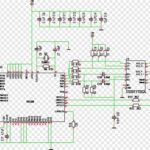
The first step in PCB manufacturing is designing the circuit and creating a layout. This is done using specialized PCB design software, such as Altium Designer, Eagle, or KiCad. The designer determines the placement of components, routing of traces, and the overall dimensions of the board.
Step 2: PCB Fabrication
Once the PCB design is finalized, the fabrication process begins. This involves several sub-steps:
-
Material preparation: The FR 4 substrate is cut to the required size and cleaned to remove any contaminants.
-
Copper cladding: A thin layer of copper is laminated onto the FR 4 substrate using heat and pressure. The copper layer can be applied to one or both sides of the substrate, depending on the design requirements.
-
Drilling: Holes are drilled into the PCB to accommodate through-hole components and vias. The drilling process is typically done using CNC (Computer Numerical Control) machines for precision and accuracy.
-
Plating: The drilled holes are plated with copper to create electrical connections between the layers of the PCB. This is done using an electroplating process.
-
Etching: The unwanted copper is removed from the PCB using a chemical etching process. This leaves behind the desired copper traces and pads.
-
Solder mask application: A layer of solder mask is applied to the PCB to protect the copper traces and prevent short circuits. The solder mask also provides a surface for printing component labels and other markings.
-
Silkscreen printing: The final step in PCB fabrication is silkscreen printing, where component labels, logos, and other markings are printed onto the solder mask.
Step 3: PCB Assembly
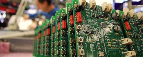
After the PCB is fabricated, the components are mounted onto the board. This can be done using two methods:
-
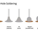
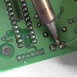
Through-hole assembly: Through-hole components are inserted into the drilled holes and soldered onto the PCB manually or using wave soldering machines.
-
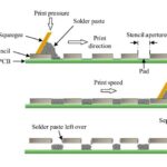
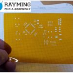
Surface mount assembly: Surface mount components are placed onto the pads on the PCB using pick-and-place machines and then soldered using reflow ovens.
Step 4: PCB Testing and Inspection
The assembled PCBs undergo various tests and inspections to ensure their quality and functionality. Some common tests include:
-
Automated Optical Inspection (AOI): An automated camera system checks for any visible defects, such as missing components, wrong component placement, or solder bridges.
-
X-ray Inspection: X-ray machines are used to inspect the internal structure of the PCB, particularly for hidden solder joints and vias.
-
In-Circuit Testing (ICT): An ICT machine probes the PCB and checks for any shorts, opens, or other faults in the circuit.
-
Functional Testing: The PCB is powered up and tested for its intended functionality to ensure it meets the design specifications.
Factors Affecting FR 4 PCB Manufacturing Quality
Several factors can affect the quality of FR 4 PCBs during the manufacturing process. Some of these factors include:
Material Quality
The quality of the FR 4 substrate and copper foil used in PCB manufacturing can significantly impact the final product’s performance. Poor quality materials may lead to issues such as delamination, warping, or poor electrical properties.
Manufacturing Process Control
Strict process control is essential to ensure consistent quality in PCB manufacturing. This includes maintaining proper temperatures, pressures, and exposure times during lamination, plating, and etching processes. Any deviations from the optimal process parameters can result in defects or reduced performance.
Environmental Control
PCB manufacturing facilities must maintain a clean and controlled environment to prevent contamination and ensure product quality. This includes controlling factors such as temperature, humidity, and airborne particles.
Operator Skill and Training
The skill and training of the operators involved in PCB manufacturing can also affect the quality of the final product. Proper training and adherence to standard operating procedures are essential to minimize human errors and ensure consistent results.

Advancements in FR 4 PCB Manufacturing
As the demand for high-performance electronics continues to grow, there have been several advancements in FR 4 PCB manufacturing to meet these challenges.
High-Frequency Materials
With the increasing use of high-frequency applications, such as 5G networks and millimeter-wave radar, there is a need for PCB materials that can support these frequencies. High-frequency FR 4 variants, such as FR 4.7 and FR 4.8, have been developed to offer better signal integrity and lower dielectric loss at higher frequencies.
Embedded Components
Embedded component technology involves mounting components within the layers of the PCB rather than on the surface. This can lead to smaller board sizes, improved signal integrity, and better thermal management. Advances in FR 4 materials and manufacturing processes have made embedded component PCBs more feasible and cost-effective.
Multilayer PCBs
Multilayer PCBs consist of multiple layers of FR 4 substrates laminated together, with copper traces and vias connecting the layers. Advances in multilayer PCB manufacturing have enabled the production of boards with higher layer counts, finer trace widths, and smaller via sizes. This allows for more complex designs and higher component densities.
Flexible and Rigid-Flex PCBs
Flexible PCBs are made using flexible substrates, such as polyimide, while rigid-flex PCBs combine both rigid FR 4 and flexible substrates. These types of PCBs offer greater design flexibility and can be used in applications where the board needs to conform to a specific shape or withstand repeated bending. Advances in materials and manufacturing processes have made flexible and rigid-flex PCBs more reliable and cost-effective.
Environmental Considerations in FR 4 PCB Manufacturing
As with any manufacturing process, PCB production can have an impact on the environment. There are several environmental considerations that must be taken into account when manufacturing FR 4 PCBs.
Hazardous Materials
Some of the chemicals used in PCB manufacturing, such as etchants and plating solutions, can be hazardous to human health and the environment if not handled properly. PCB manufacturers must follow strict regulations and guidelines for the use, storage, and disposal of these materials to minimize their environmental impact.
Waste Management
PCB manufacturing generates various types of waste, including scrap PCBs, copper waste, and chemical waste. Proper waste management practices, such as recycling and treatment, are essential to reduce the environmental impact of PCB production.
Energy Consumption
PCB manufacturing processes, such as lamination and Reflow Soldering, consume significant amounts of energy. Implementing energy-efficient equipment and practices can help reduce the environmental footprint of PCB production.
Green Materials
There is a growing trend towards the use of environmentally friendly materials in PCB manufacturing. This includes the use of halogen-free FR 4 substrates, lead-free solders, and water-based cleaning agents. These materials can help reduce the environmental impact of PCB production without compromising performance.
Future Trends in FR 4 PCB Manufacturing
As technology continues to advance, there are several future trends that are likely to shape the FR 4 PCB manufacturing industry.
Miniaturization
The demand for smaller and more compact electronic devices is driving the trend towards miniaturization in PCB manufacturing. This includes the use of smaller components, finer trace widths, and higher layer counts to achieve higher component densities and smaller board sizes.
3D Printing
3D printing technology has the potential to revolutionize PCB manufacturing by enabling the production of complex, three-dimensional structures. This could include the printing of conductive traces, insulating substrates, and even embedded components. While still in the early stages of development, 3D-printed PCBs could offer greater design flexibility and faster prototyping.
Automation and Industry 4.0
The adoption of automation and Industry 4.0 technologies, such as robotics, artificial intelligence, and the Internet of Things (IoT), is expected to increase in PCB manufacturing. These technologies can help improve process control, reduce human errors, and increase efficiency and productivity.
Sustainable Manufacturing
There is a growing emphasis on sustainable manufacturing practices in the PCB industry. This includes the use of renewable energy sources, the implementation of closed-loop water systems, and the adoption of circular economy principles to minimize waste and maximize resource efficiency.
Frequently Asked Questions (FAQ)
-
What is the difference between FR 2 and FR 4 PCBs?
FR 2 PCBs are made using phenolic resin, while FR 4 PCBs use epoxy resin. FR 4 PCBs offer better mechanical and electrical properties compared to FR 2, making them suitable for a wider range of applications. -
Can FR 4 PCBs be used for high-frequency applications?
Standard FR 4 PCBs may not be suitable for very high-frequency applications due to their dielectric properties. However, high-frequency FR 4 variants, such as FR 4.7 and FR 4.8, have been developed to offer better performance at higher frequencies. -
What is the maximum number of layers possible in an FR 4 PCB?
The maximum number of layers in an FR 4 PCB depends on the manufacturer’s capabilities and the specific design requirements. Some manufacturers can produce PCBs with up to 50 layers or more. -
How can I ensure the quality of FR 4 PCBs from a manufacturer?
To ensure the quality of FR 4 PCBs, choose a manufacturer with a proven track record and quality certifications, such as ISO 9001 and UL. Request documentation, such as material certifications and test reports, to verify the quality of the materials and processes used. -
Are FR 4 PCBs environmentally friendly?
Standard FR 4 PCBs may contain hazardous materials, such as halogens, which can have an environmental impact. However, there are environmentally friendly options available, such as halogen-free FR 4 substrates and lead-free solders. Additionally, proper waste management and recycling practices can help reduce the environmental footprint of PCB manufacturing.
Conclusion
FR 4 PCB manufacturing is a complex process that involves several steps, from design and fabrication to assembly and testing. The quality of FR 4 PCBs is influenced by various factors, such as material quality, process control, environmental control, and operator skill. Advancements in FR 4 PCB manufacturing, such as high-frequency materials, embedded components, and multilayer PCBs, have enabled the production of more complex and high-performance boards.
Environmental considerations, such as hazardous materials, waste management, and energy consumption, are also important aspects of FR 4 PCB manufacturing. The adoption of green materials and sustainable manufacturing practices can help reduce the environmental impact of PCB production.
Looking to the future, trends such as miniaturization, 3D printing, automation, and sustainable manufacturing are expected to shape the FR 4 PCB manufacturing industry. As technology continues to advance, PCB manufacturers will need to adapt and innovate to meet the evolving demands of the electronics industry while minimizing their environmental footprint.
Leave a Reply