Introduction
Fabrication boards and printed circuit boards (PCBs) are a foundational component of electronic product design. Optimizing the design of boards is crucial to delivering high product performance and reliability. This article explores key techniques for fabrication board design, from layout considerations to part selection, copper thickness, and beyond. Follow best practices in PCB design to ensure your next product shines.
Selecting the Right Fabrication Board Materials
Choosing the right board materials is the first step in optimizing PCB design. Consider factors such as:
Dielectric Type
Popular dielectrics include FR-4, polyimide, PTFE, and ceramic-filled PTFE. FR-4 glass epoxy is economical while polyimide and PTFE offer superior thermal and dielectric performance for high-frequency applications. Just ensure your PCB fabrication partner can work with your chosen dielectric.
Copper Thickness
Thicker copper provides lower electrical resistance while thinner copper allows for finer traces and spacing. Common thicknesses are 1oz (35μm), 2oz (70μm), and 3oz (105μm).
Thicker plating/copper layers also improves heat dissipation.
Number of Layers
More layers allow for shorter traces and better isolation of signals. 4-6 layers are common. High-performance designs may use 20+ layers.
Board Thickness
Standard thickness is 1.6mm (FR-4) but can range from 0.4mm to over 5mm. Thicker boards are sturdier but limit component height.
| Parameter | Options | Considerations |
|---|---|---|
| Dielectric Type | FR-4, Polyimide, PTFE/ceramic-filled PTFE | Electrical performance, cost |
| Copper Thickness | 1oz, 2oz, 3oz+ | Conductivity vs. trace spacing |
| Number of Layers | 2-4 (budget), 4-20+ (high-performance) | Routing complexity, signal isolation |
| Board Thickness | 0.4mm – 5mm+ | Strength vs. component clearance |
Use this table to select PCB materials tuned for your specific performance, reliability, and cost requirements.
Optimizing the Physical Board Layout
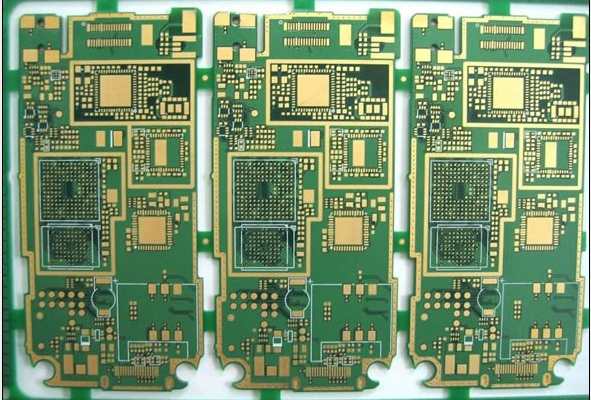
Careful board layout is critical for achieving design goals like high signal integrity, thermal performance, and manufacturability. Follow these PCB layout best practices:
Follow Design Rules and Constraints
Work closely with your fabrication shop to establish design rules for:
- Minimum trace width/spacing
- Annular rings around plated through-holes
- Solder mask web thickness
- Via styles and anti-pad dimensions
- Impedance control (if needed)
Follow all specified design rules and constraints to ensure manufacturability. Leave room for adjustments later if possible.
Partition and Isolate Functional Blocks
Group related circuits together and isolate them using ground planes as shields. This contains electromagnetic interference (EMI) and prevents cross-talk. Keep analog and digital circuits well separated.
Use Planes and Solid Polygons for Ground and Power
Flooding unused areas with copper polygons connected to ground or power nets improves EMI rejection and thermal performance. Use an entire layer as a ground or power plane if possible.
Place Decoupling Capacitors Close to ICs
Each IC power pin should have an adjacent decoupling capacitor. Place them as close to the IC as possible using short direct traces. Vias to power/ground planes are ideal. This provides charge locally, preventing power rail noise.
Route Traces Orthogonally
Use mainly horizontal and vertical traces. 45 and 135 degree traces complicate routing and can cause reflections degrading signal integrity at higher frequencies.
These guidelines help optimize the physical PCB layout for electrical performance, thermal management, and easy assembly.
Selecting the Right Components
Component selection also affects the performance of your finished board. Follow these tips:
Choose Components Rated for Board Temperature
Ensure all components are rated to withstand soldering temps and the board’s internal operating temperature. De-rate max temps by 10-15C for margin.
Prefer SMT Packages When Possible
Surface mount packages take up less space than through-hole, allow for automation, and make hand assembly easier. Some key SMT packages:
- 0402, 0603, 0805, 1206, 1210 resistors and caps
- SOIC, SSOP, QFP, BGA ICs
- SOT-23 FETs
Minimize IC Pin Counts
Choosing ICs with fewer pins simplifies routing. Avoid BGAs with high pin counts if possible.
Check Component Heights
Tall components can interfere with board assembly and clearance inside enclosures.
Use Generous Footprint Sizing
Use footprint sizes close to maximum component dimensions for easier hand assembly and inspection.
Ensure Parts are Available in Volume
Confirm parts spec’d for your board are available in volume from suppliers before finalizing the design. Perform risk assessments on hard to source components.
Choosing the right SMT packages, minimizing pin counts, and planning for manufacturability reduces headaches during board assembly and rework.
Further Optimizations
Additional techniques to optimize fabrication board performance include:
- Impedance Control: Match trace widths and distances between planes to achieve target impedance for high speed signals
- High-Speed Routing: Minimize vias, use blind/buried vias, eliminate stubs, match trace lengths
- EMI Mitigation: Use shielding, filtering, proper grounding, and specialized EMI-resistant components
- Thermal Management: Incorporate thermal vias, copper-filled polygons, and consider adding a backplate or heatsink
- DFM: Design for ease of fabrication and assembly. Allow room for adjustments.
Optimizing Fabrication and Assembly
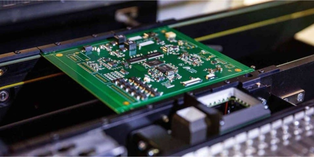
Work with your fabrication shop to ensure your design is optimized for their capabilities:
- Share your IPC Class 2 vs. 3 requirements
- Confirm minimum feature sizes and available layer counts
- Verify their offered soldermask expansion tolerances
- Check if they allow via-in-pad, microvias, or impedance control
- Review their design rules manual or work with an applications engineer
Avoid surprises by matching your design to your specific PCB fabricator’s capabilities.
Conclusion
Optimizing fabrication board design requires careful consideration of materials, layout practices, component selection, high-speed design techniques, thermal management, and manufacturability. Working closely with your PCB vendor ensures your design aligns with their process limitations. Following the guidelines in this article will help you maximize the performance and reliability of your next PCB design.
Frequently Asked Questions
What are some key factors to consider when selecting a PCB material?
Some key considerations are dielectric type, copper weight, number of layers, and board thickness. Select a dielectric such as FR-4 or polyimide suited for your required electrical performance. Heavier copper improves conductivity while thinner copper enables tighter trace spacing. Choose layer count based on routing complexity and isolation needs. Consider thermal dissipation requirements when selecting board thickness.
How can I contain EMI and cross-talk in my PCB design?
Use ground planes between functional blocks for shielding. Route sensitive traces away from noisy ones or use ground guards. Eliminate stubs, use impedance control, and avoid 45/135 degree traces. Choose components with low radiation and high immunity. Incorporate shielding, filtering, and proper board-level grounding.
What design practices help enable easy board assembly?
Use mainly surface mount components with larger package sizes. Minimize BGAs pin counts. Allow room between components for inspection and rework. Use generous footprint sizes close to component max dimensions. Ensure parts are available for volume production. Design to your fabrication shop’s assembly capabilities.
What are some key thermal management strategies for PCBs?
Incorporate thermal vias under hot components to conduct heat to inner or back side layers. Connect those layers to large copper polygons tied to ground to act as heat sinks. Use the maximum number of copper layers possible. Consider adding a backplate or heatsink if component power dissipation is very high. Ensure adequate airflow over the board.
How can I avoid issues during PCB fabrication and assembly?
Review your fabrication shop’s design rules manual and work with their application engineers. Follow all specified design rules and share your IPC Class 2 vs. 3 requirements. Confirm they can fabricate all features in your design, including advanced via structures. Make adjustments where needed to align with their process capabilities.
Leave a Reply