Introduction
Printed circuit boards (PCBs) are essential components of nearly all modern electronics. From computers and smartphones to advanced medical devices, PCBs provide the foundation on which components are mounted and connected. As electronics grow more complex, so too do the demands on PCBs. This is where elic PCBs come in.
Elic PCBs utilize the latest in design and manufacturing techniques to create boards that meet the needs of today’s cutting-edge electronics. In this article, we’ll take a close look at elic PCB fabrication and assembly. We’ll examine what makes elic PCBs unique, the specialized techniques used to fabricate them, and the assembly process that turns bare boards into functional circuits.
What Are Elic PCBs?
Elic PCBs represent the highest quality tier of printed circuit boards on the market today. They go far beyond the capabilities of standard PCBs to offer:
- Extremely high component densities
- More board layers (up to 30+ layers)
- Finer lines/spaces (trace widths and distances down to 2/2 mil)
- Advanced materials like ceramic substrates
- Complex designs like HDI (High Density Interconnect)
- Rigorous quality control standards
This combination of design complexity and precision manufacturing allows elic PCBs to meet the needs of leading-edge electronic devices. Applications include:
- High-speed computing (servers, supercomputers)
- Networking/telecom equipment
- Aerospace/defense systems
- Medical electronics
- Automotive electronics
In short, elic PCBs provide the sophisticated circuit foundation necessary for today’s most advanced electronics. Their specialized fabrication empowers miniaturization and performance beyond what’s possible with standard PCBs.
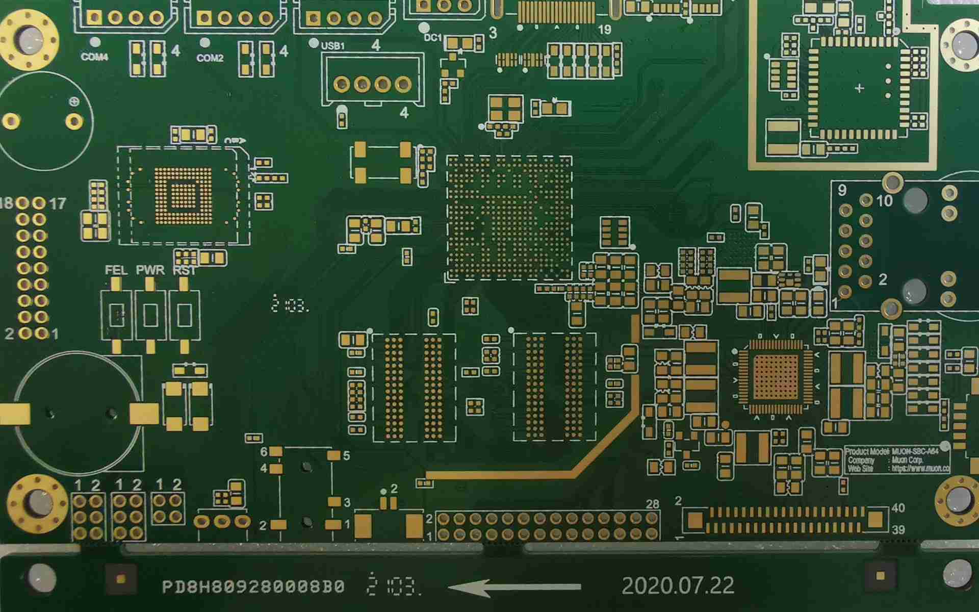
Elic PCB Fabrication
Fabricating elic PCBs requires specialized techniques and precision production capabilities. Here are some of the key manufacturing processes involved:
Layer Stackup
Elic PCBs can have many more conductive layers than standard boards thanks to advanced layer stackup designs. While everyday PCBs typically have just 2 or 4 layers, elic PCBs often have 12, 16, 20, or even 30+ layers.
These additional layers are embedded within the board itself and connected using microvias (tiny vertical interconnects between layers). The layer stackup allows elic PCBs to accommodate extremely high component densities.
Thin Dielectrics
The material that separates the conductive layers is called dielectric material. Elic PCBs use new ultra-thin dielectrics that are just 2-3 microns thick. Compare this to 50+ microns for standard PCB dielectrics.
Thinner dielectrics allow layers to be packed more closely together, enabling finer routing traces and more layers within a given thickness.
Laser Drilling
Microvias that interconnect layers are created using laser drilling. The laser drilling process can produce tiny vias just 6-10 microns (0.006 mm) in diameter. The use of microvias further boosts component density.
Laser drilling also allows the use of “blind” and “buried” vias that connect specific inner layers without going all the way through the full layer stackup. This facilitates dense routing.
Fine Lines/Spaces
Elic PCBs leverage advanced photolithographic processes to create incredibly fine lines and spaces. Traces and distances between traces can be as small as 2 mils (0.002 inches). This is 6-10X finer than standard PCBs, resulting in further miniaturization.
Advanced Materials
Standard PCB substrate materials like FR-4 have limitations in electrical performance, thermal conductivity and dimensional stability. Elic PCBs turn to advanced substrate materials like:
- High-frequency laminates for improved signal integrity at high speeds
- Ceramic substrates for maximum thermal performance
- Composite epoxy blends for enhanced dimensional stability
These materials provide the performance essential to support elic PCB density and design complexity.
Rigorous Testing
Throughout the fabrication process, elic PCBs undergo extensive electrical, mechanical and environmental stress testing. This includes automated optical inspection (AOI), x-ray inspection, network analysis and rigorous quality control checks.
Strict process controls and comprehensive testing ensures elic PCBs meet the highest standards of quality and reliability.
Elic PCB Assembly
The fabrication process produces the raw elic PCB with all conductive traces and layers. To create a functioning electronic circuit, components must be assembled onto the bare board through placement and soldering.
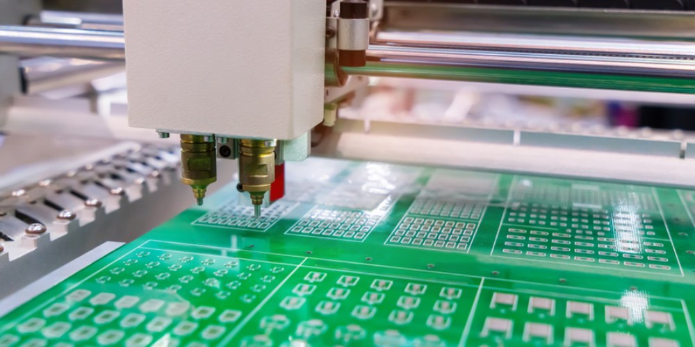
SMT Assembly
The majority of components are assembled onto elic PCBs using surface mount technology (SMT). This involves robotic pick-and-place machines precisely positioning each component and soldering it in place.
SMT enables extremely high component densities, with chip-scale packages and microscopic 01005 passives readily accommodated. The placement machines feature advanced vision alignment systems for precision down to 50 microns.
Reflow Soldering
Reflow soldering melts solder paste deposited on SMT pads to electrically attach components. The elic PCB panel passes through a multi-zone reflow oven with tightly controlled temperature profiles. The process ensures reliable solder joints without damaging sensitive board or component materials.
Selective Soldering
For components unsuitable for SMT like connectors or transformers, elic PCB assembly uses selective wave soldering. This locally applies solder just to selected through-hole pads without exposing heat-sensitive areas.
Conformal Coating
Once assembled, elicit PCBs will often receive a protective conformal coating. The thin lacquer coating prevents environmental contamination and leakage currents across the densely-packed board.
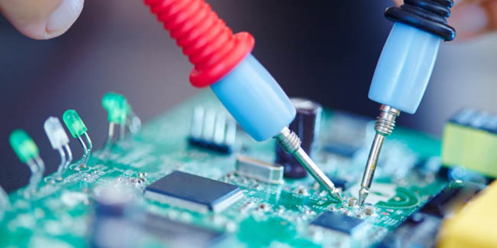
Testing/QC
Like fabrication, PCB assembly undergoes intensive inspection and testing. Automated optical inspection and x-ray check for missing or defective components. Flying probe or bed-of-nails fixtures verify electrical connectivity.
Rigorous testing ensures each completed elic PCB assembly meets performance requirements before shipping.
When Are Elic PCBs Necessary?
With their specialized design and manufacturing requirements, elic PCBs are recommended for applications meeting some or all of these criteria:
- High component density (1000+ components)
- Fine lines/spaces under 5 mils
- High layer counts (>16 layers)
- Multiple voltages required (e.g. 3.3V, 1.8V, 1.5V)
- High pin count components like FPGAs
- Extremely high speeds (25+ Gbps signaling)
- High power density requirements
- Complex power distribution needs
- Size constraints requiring IC-scale footprint
For applications like these, the elic PCB fabrication and assembly process is necessary to create boards that offer the routing density, layered design, electrical performance and reliability required.
While elic PCBs carry higher costs than standard boards, their capabilities unlock performance levels and miniaturization simply not achievable with conventional PCB technology. For advanced electronics pushing the envelope, elic PCBs provide the sophisticated circuit foundation needed for success.
Frequently Asked Questions
What are some key features of elic PCBs?
Some key features of elic PCBs include:
- Many more layers (30+ layers possible)
- Extremely dense component layouts
- Very thin dielectrics (2-3 microns)
- Microvias for vertical interconnections
- Fine trace widths/spaces down to 2 mils
- Advanced substrate materials like ceramics
- Rigorous testing and quality control
How are elic PCBs different from standard PCBs?
Elic PCBs differ from standard PCBs in their complexity, precision and performance. They have finer features, more layers, advanced materials and undergo more stringent manufacturing controls to meet the needs of cutting-edge electronics.
Why are elic PCBs important for advanced electronics?
The complexity of today’s electronics demands PCBs that can deliver sophisticated circuitry and electrical performance beyond standard boards. Elic PCBs provide the routing density, speed, power and reliability needed for applications like networking, telecom, defense, aerospace, and medical electronics.
What are some key steps in fabricating elic PCBs?
Key elic PCB fabrication steps include complex layer stackups, laser drilling of microvias, ultra-thin dielectrics, photolithography to produce fine lines/spaces, and utilization of advanced substrate materials. Each step aims to enable elic PCBs’ high performance and precision.
How does elic PCB assembly compare to standard PCB assembly?
Elic PCB assembly leverages advanced techniques like high-precision SMT pick-and-place, reflow soldering, selective wave soldering and conformal coating optimized for elic PCBs’ dense, complex designs. Rigorous testing also verifies assembly quality.


Leave a Reply