Introduction
Printed circuit boards (PCBs) form the backbone of modern electronics. From computers and smartphones to medical devices and automobiles, PCBs provide the interconnects between components and integrate them into functioning circuits and systems. While single-sided PCBs can suffice for simple designs, complex products often require double sided PCBs to achieve higher component density and interconnect capability. This article provides a comprehensive guide to double sided PCB assembly.
What is a Double Sided PCB?
A double sided PCB has conductive traces patterned on both sides of the board, allowing components to be placed and interconnected on both sides. This effectively doubles the available area for traces and components compared to a single-sided board. Vias or plated through holes electrically connect the top and bottom layers to complete circuits between components on both sides. The main advantages of double sided PCBs are:
- Higher component density: More space for component placement and routing traces on two layers instead of one.
- Shorter traces: Components can be placed closer together, enabling shorter trace lengths for faster signal speeds.
- Lower layer counts: Functionality achievable with fewer conductive layers compared to multilayer boards.
- Cost effectiveness: Lower cost compared to multilayer boards for many applications.
Double sided boards are the minimum configuration for complex digital circuits, mixed-signal designs involving both analog and digital signals, and high component density applications like cell phones and handheld devices. They provide a good balance between capability and affordability.
Double Sided PCB Design Considerations
Designing a double sided PCB requires careful planning to utilize the advantages of the two-layer configuration efficiently. Here are some key considerations:
Component placement: Optimal component placement is crucial, with related circuits grouped together to minimize interconnect distances. Mixed-signal circuits should segregate analog and digital sections.
Routing channels: Routing channels between sections should be allocated appropriately to route traces on both layers. Wider channels may be required in high-density areas.
Layer usage: Each layer can have defined roles, e.g. one for power distribution and one for signals. This separation helps reduce noise.
Via placement: Vias should be placed judiciously to transition traces between layers at optimal junctures with minimal jogging. Too many vias can be problematic.
Split planes: Partial ground or power planes on each layer connected by vias helps decouple noise while allowing routing space.
Balancing layers: Ensure trace densities are balanced between layers for even stress and warp characteristics.
Thermal management: Provide thermal relief cutouts, pads, and sufficient ground plane area for heat dissipation.
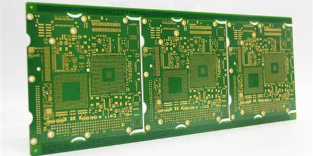
Double Sided PCB Fabrication Process
Double sided PCB fabrication involves creating conductive layers on both sides of the substrate and drilling/plating through-hole vias to interconnect them. The basic fabrication steps are outlined below:
Step 1 – Preparation
The fabrication process starts with an FR-4 glass epoxy substrate about 1.6mm thick. The substrate panels are cleaned, coated with an adhesion promoter, then coated with photoresist.
Step 2 – Imaging
The artwork for the conductive pattern on each layer is imprinted onto the photoresist using lithography techniques. For the top side, the panel is exposed to UV light through the artwork transparency. The bottom side is aligned precisely and then exposed.
Step 3 – Developing
The panel goes through a chemical developing process to remove the unexposed photoresist, leaving behind the desired conductive pattern on both sides protected by photoresist.
Step 4 – Etching
The exposed copper is corroded away using etching chemicals, resulting in the isolated copper traces of the printed circuit left behind.
Step 5 – Stripping
The remaining photoresist is stripped away, resulting in the completed conductive pattern on both sides.
Step 6 – Via Formation
Holes are precisely drilled through the board at via locations. The walls of the holes are plated with copper to form the vias.
Step 7 – Finishing
The panels go through various chemical processes for cleaning, then coated with solder mask and silkscreen for identification. Boards are finally separated by routing/scoring.
| Step | Process |
|---|---|
| 1 | Substrate Preparation |
| 2 | Imaging |
| 3 | Developing |
| 4 | Etching |
| 5 | Stripping |
| 6 | Via Formation |
| 7 | Finishing |
This sequence of fabrication processes results in completed double sided PCBs ready for component assembly. The key is precision at each step to achieve fine conductors with tight tolerances.
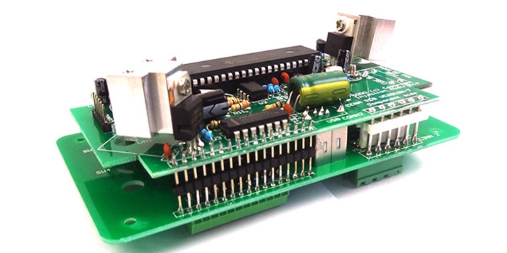
Double Sided PCB Assembly Process
Populating components onto fabricated double sided PCBs is known as PCB assembly. This involves soldering of surface mount (SMT) components and through-hole components to form the final board assembly. The assembly steps are:
Step 1 – Solder Paste Application
Solder paste is applied on SMT pad locations on both sides through screen printing or jetting. For boards with fine pitches, solder spheres are used.
Step 2 – SMT Component Placement
SMT components are accurately placed onto their pads on the bottom side first using pick-and-place machines. The board is then flipped over and components are mounted on the top side.
Step 3 – Reflow Soldering
The board passes through a reflow oven causing the solder paste to melt, securely soldering the SMT components in place on both sides.
Step 4 – Through-Hole Component Insertion
Components with leads are inserted into their corresponding holes from the proper side.
Step 5 – Wave Soldering
The board underside passes over a wave of molten solder, soldering the leads of through-hole components.
Step 6 – Cleaning/Inspection
Flux residue is cleaned off and boards are visually inspected or use automated optical inspection.
Step 7 – Programming/Testing
For microcontroller boards, the chip firmware is loaded. All boards undergo functional testing.
| Step | Process |
|---|---|
| 1 | Solder Paste Application |
| 2 | SMT Component Placement |
| 3 | Reflow Soldering |
| 4 | Through-Hole Component Insertion |
| 5 | Wave Soldering |
| 6 | Cleaning/Inspection |
| 7 | Programming/Testing |
This sequence results in a fully assembled and tested double sided PCB ready for use in products. With attention to quality control at each step, the result is a reliable PCB assembly.
Key Takeaways on Double Sided PCBs
Here are the main points on double sided PCB technology:
- Provides 2-layer interconnects for higher component densities than single-sided boards.
- Vias interconnect the top and bottom conductive layers.
- Careful design is needed to effectively utilize both sides.
- Fabrication uses lithography to pattern both sides and plated vias.
- Assembly solders SMT and through-hole components onto both sides.
- Enables complex, compact, and cost-effective PCB solutions.
- Balances capability and affordability between single-sided and multilayer boards.
- Extensively used across consumer and industrial electronics.
FAQ
Here are answers to some frequently asked questions about double sided PCB assembly:
Q: What are typical substrate thicknesses for a double sided PCB?
A: Standard substrate (base material) thicknesses range from 0.4mm to 2.0mm, with 1.6mm being the most common. Thinner substrates are used in space constrained applications.
Q: What are the minimum trace widths and spaces possible on double sided PCBs?
A: Using advanced fabrication techniques, trace widths and spaces down to 3-5 mils (0.15mm) are achievable on double sided boards. Even finer geometries are possible with HDI processes.
Q: How many routing layers are possible in a double sided PCB?
A: Strictly speaking, there are only two signal layers – top and bottom conductive layers. However, split power or ground planes can be used for some pseudo-layer routing.
Q: What are typical via diameters on double sided PCBs?
A: Standard via diameters range from 10-12 mils (.25-.3mm). Microvias with diameters below 8 mils are also possible with advanced processes.
Q: What components are typically used on double sided PCB assemblies?
A: A mix of surface mount (SMT) parts like resistors, capacitors, ICs and through-hole components like connectors, large ICs are used. High density designs maximize SMT usage.


Leave a Reply