Blind vias are an important component in printed circuit board (PCB) design and manufacturing. As the name suggests, blind vias connect layers on a PCB without going all the way through from the top to the bottom. Understanding the costs associated with blind vias is key for PCB designers and fabricators. In this comprehensive guide, we’ll look at what blind vias are, why they are used, their cost implications, and how to optimize your design to balance performance and cost when using blind vias.
What are Blind Vias?
A via is a plated through hole (PTH) that connects two or more layers in a PCB. Vias can either go all the way through the PCB from top to bottom (through vias) or only connect internal layers without reaching the outer surfaces (blind/buried vias).
Blind vias start on an outer layer but only connect to one or more inner layers without penetrating to the other side. In contrast, buried vias connect two or more inner layers only, without connecting to either outer surface.
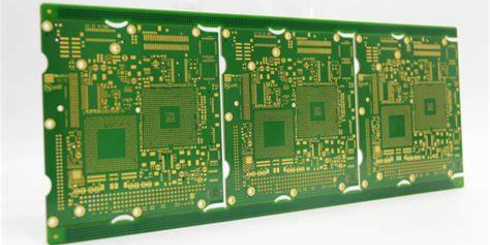
A blind via connecting an outer layer to inner layers
Blind and buried vias are often used when routing high-speed signals or for RF designs. They allow connections between layers that minimize stub effects or crosstalk compared to using through vias. As we’ll see, there are cost tradeoffs for the improved performance.
Why Use Blind Vias?
There are several reasons blind and buried vias are used instead of through vias:
- Signal integrity – Blind vias have much smaller stubs than through vias, improving signal quality for high-speed signals. The shorter stub acts as a smaller capacitor, reducing impedance discontinuities.
- Component placement – Using blind/buried vias allows flexibility in component placement. Connections can be made between non-adjacent layers.
- Noise isolation – Blind vias help isolate noise between sections of a PCB. Sensitive analog signals can be routed on inner layers separately from noisy digital signals.
- Form factor – Products with space constraints can use blind/buried vias to route connections without requiring vias to go through the entire board.
- Improved manufacturability – Buried vias allow connections without using up space for through-via pads on outer layers. This helps maximize routing space.
The benefits of reduced parasitics, noise isolation, and flexible routing often make blind/buried vias worth the additional costs compared to through vias. When designing high-frequency or compact boards, they are an essential part of a successful implementation.
Blind Via Cost Factors
Several factors contribute to the fabrication costs when using blind and buried vias:
1. Layer Count
The number of PCB layers directly impacts the blind via cost. A 4-layer board is the simplest case for using them. But higher layer counts allow more complex blind/buried connections with potentially greater benefits. However, each additional layer adds costs.
Going from a 4-layer to 6-layer PCB often has around a 30% cost increase. The increase from 6 layers to 8 layers can be 50% or more. Some of this incremental cost is due to the blind vias themselves.
2. Stackup Design
The stackup design also influences cost. Having blind/buried vias between layers grouped closely together is cheaper compared to spacing them over several layers. For example, vias between Layers 1-3 are simpler than vias between Layers 1-6.
3. Via Process Steps
The steps to form blind vias add complexity versus plating through vias:
- Laser drilling each blind via depth
- Precise depth control to reach target layers
- Separate metallization and plating steps for each layer pair
- Filling voids to avoid trapped air pockets
More processing means higher costs.
4. Registration Accuracy
Blind vias require very accurate alignment between layers. The via barrel on each layer must line up precisely. This depends on tight process controls and registration. Misalignment can cause opens or reliability issues.
5. Test and Inspection
Verifying plating uniformity and connections for blind/buried vias requires detailed electrical testing and x-ray inspection. This adds cost compared to simpler through-via testing.
6. Yield Losses
All the above factors can contribute to lower yields versus simpler PCBs without blind/buried vias. Any failed boards are discarded, driving up average costs.
Estimating Blind Via Costs
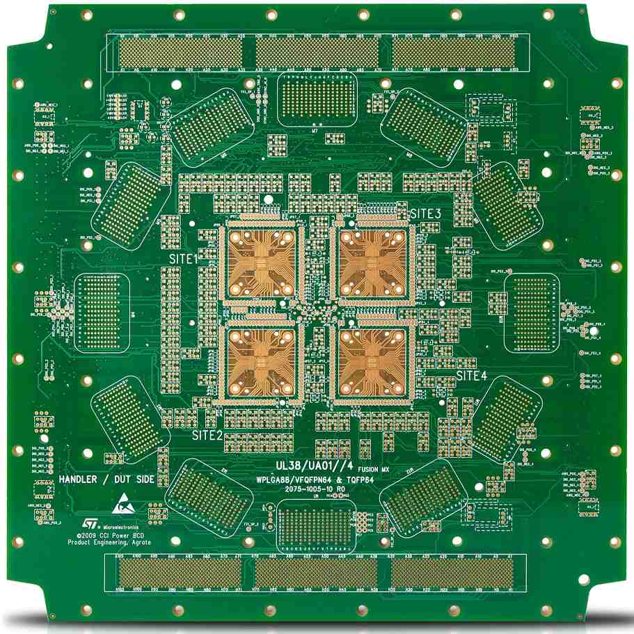
As a rough estimate, a 4-layer PCB with a few blind vias may cost 5-10% more than an equivalent board using only through vias. On higher layer count boards, the blind via costs are a larger portion of the overall expense.
According to one study by EMA Design Automation, moving from a 12-layer to 20-layer PCB increased price by 3x. The blind and buried vias contributed to 40% of that cost increase.
For a production volume board, adding 2-4 blind via layers might increase cost by 25-50% over using just through vias. At the prototype stage, small quantities magnify the costs further.
To get accurate pricing, it’s best to get quotes from fabricators. The designs can be optimized to balance performance and costs.
Cost Optimization Tips
Here are some tips to optimize use of blind/buried vias and control costs:
- Carefully consider layer count – Add layers only as needed, as each increases costs.
- Group related layers – Minimize blind/buried via depths.
- Share vias when possible – Use one via to route multiple signals if layout permits.
- Limit high-density areas – Spread out routing if possible, rather than localize vias in one area.
- Ask about panelization – Grouping boards may improve fabrication pricing.
- Compare fabricators – Get quotes from multiple vendors. Prices can vary widely.
- Evaluate materials – Standard FR-4 is lowest cost. High-performance materials add expense.
- Order prototypes – Validate designs before high-volume manufacturing.
- Review DFM recommendations – Follow fabricator guidelines for max yield.
- Communicate with your fabricator – Discussing optimizations can help reduce costs.
When Do Blind Vias Make Sense?
Given the additional costs, blind vias should be used judiciously where their benefits outweigh the expense. Here are typical application cases where they are worth considering:
- High layer count complex boards (8+ layers)
- High-speed digital logic with fast edge rates
- RF boards with signals above several GHz
- Very dense board layouts with component clearance issues
- Noise isolating certain circuitry is mandatory
- Stackup/form factor constraints require non-adjacent layer connections
For simpler, low-frequency boards blind vias may not justify the costs. But for many advanced designs, the performance or layout benefits make them indispensable, even with the increased fabrication pricing.
Conclusion
While blind and buried vias come with increased costs compared to through vias, they enable high-performance PCB designs with improved signal integrity and noise control. When used appropriately for complex multilayer boards, the benefits typically outweigh the fabrication expense increases of 10-50% or more compared to equivalent all-through-via designs.
By optimizing layer stackups, sharing vias when possible, and working closely with your PCB supplier, the costs of blind vias can be managed. For cutting-edge circuit designs, the performance advantages mean blind vias are an essential part of the PCB technology arsenal.
Frequently Asked Questions
What is the main cost factor for blind vias?
The number of layers is the largest contributor to blind via costs. Each additional layer increases fabrication complexity and price. Other factors like process steps, alignment accuracy, and testing also add cost but are secondary to layer count.
When does it make sense to use blind vias?
Blind vias provide the most benefit for high-speed digital, RF, and other demanding circuit applications, usually on boards with 8 or more layers. Their superior signal integrity outweighs the higher costs for these types of designs. On simpler boards, through vias may be adequate at lower prices.
Can I estimate how much blind vias will add to PCB cost?
As a rough estimate, a 4-layer board might see a 5-10% increase with a few blind vias versus all through vias. On higher layer count boards, the cost increase could be 25-50% or more depending on the via quantities and layout complexity. Quotes from fabricators will give more accurate pricing.
How can I reduce the cost impact of using blind vias?
Ways to minimize blind via costs include optimizing layer stackups, sharing vias when layout permits, limiting use to required areas, comparing fabricator pricing, and following all design rules and DFM guidelines. Communication with your PCB supplier is key.
When is it better to use microvias instead of blind vias?
Microvias take up less space on routing layers since they laser drill after lamination. But they require specialized processes that increase costs further. They can make sense when blind vias consume too much routing area due to pad sizes, at the expense of higher prices.

Leave a Reply