Introduction to DesignSpark PCB
DesignSpark PCB is a powerful yet easy-to-use printed circuit board (PCB) design software for Windows computers. Developed by RS Components, DesignSpark PCB enables engineers, hobbyists, and students to quickly design professional quality PCBs for prototyping or small production runs.
Some key features of DesignSpark PCB include:
– Schematic capture and PCB layout in a single integrated environment
– Extensive library of schematic symbols and PCB footprints
– Real-time design rule checking (DRC) to prevent errors
– 3D visualization of the PCB design
– Output generation for manufacturing (Gerber, drill files, BOMs, etc.)
Best of all, DesignSpark PCB is completely free to download and use, making it an excellent choice for those getting started with PCB design or working on a tight budget. Let’s take a closer look at how to get started with DesignSpark PCB and use it to design your own custom circuit boards.
Downloading and Installing DesignSpark PCB
To get started, head over to the DesignSpark PCB product page and click the “Download Free Software” button. You’ll need to create a free DesignSpark account if you don’t already have one.
The DesignSpark PCB installer is a relatively large download at around 1GB in size. Once downloaded, run the installer and follow the prompts to install DesignSpark PCB on your Windows PC. The software requires Windows 7 or later.

DesignSpark PCB User Interface Overview
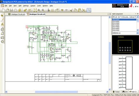
Upon launching DesignSpark PCB, you’ll be greeted by the main application window:
The user interface is divided into several key areas:
1. Menu bar – provides access to file operations, tools, view options, and help
2. Main toolbar – commonly used tools for placing parts, drawing shapes, etc.
3. Design explorer – hierarchical view of schematic pages, PCB Layers, components, nets, etc.
4. Properties panel – displays properties of the currently selected object
5. Messages panel – lists design rule violations and other notifications
6. Work area – main canvas for schematic capture and PCB layout
You can customize the user interface by dragging panels to new positions or turning panels on/off via the View menu.

Creating a New Project
To create a new DesignSpark PCB project, select File > New > Project from the menu bar. Enter a project name and location. This will create a new empty project with a single schematic sheet.
It’s a good idea to save your project at this point via File > Save. Get in the habit of saving regularly as you work on your designs.

Drawing the Schematic
Placing Parts
The first step in creating a PCB is typically drawing the schematic – a symbolic representation of the circuit’s components and connections. To start placing parts, click the Place Part button on the main toolbar or select Tools > Place > Part from the menus.
This will open the Part Browser where you can search or browse through DesignSpark PCB’s extensive library of schematic symbols. Find the desired part and double-click it or click OK to place it in the work area.
Click to place multiple copies of the part or press Esc when done. Right-click and drag to rotate or flip the part. You can also edit component properties like reference designator, value, and footprint by double-clicking the part.
Drawing Wires
To make electrical connections between component pins, use the Draw Wire tool on the toolbar or Tools > Draw > Wire from the menus. Click on a component pin as the start point, then click on the destination pin. Press Esc when done drawing wires.
Naming Nets
Wires drawn between pins define nets – uniquely named electrical connections. When a wire is first drawn it is assigned an automatically generated net name like N$1, N$2, etc.
To assign a more meaningful net name, double-click on the wire and edit the Net property. You can also rename nets in the design explorer under the Nets folder.
Proper net naming is important for readability and for defining special nets like power and ground.
Placing Power and Ground Symbols
Most schematics will have one or more power and ground nets. To place power/ground symbols, use the Place Power or Place Ground buttons on the toolbar. These symbols don’t represent physical components but rather indicate power connections to a net.
Checking the Schematic
Before proceeding to PCB layout, it’s important to carefully check the schematic for errors. Some things to look out for include:
– Missing or incorrect power/ground connections
– Unconnected component pins (unless intentional)
– Incorrect component values or footprints
– Incorrect net names
DesignSpark PCB includes an Electrical Rules Check (ERC) tool that can help find some types of schematic errors. Select Tools > Electrical Rules Check to run it. The results will be displayed in the Messages panel.
PCB Layout
Once the schematic is complete, you’re ready to start laying out the physical PCB. Select Tools > Convert to PCB to transfer the components and nets from the schematic to the PCB editor.
Specifying Board Outline and Layer Stack-up
The first step in PCB layout is typically defining the board size and shape and layer stack-up. To draw the board outline, use the Draw Board Outline tool on the toolbar. Click to define the outline vertices.
To specify the layer stack-up, select Design > Layer Stack Manager. Here you can define the number and types of layers, their order, and the board thickness. A typical simple 2-layer board might have a Top layer, Bottom layer, and two inner plane layers for power and ground:
| Layer | Type |
|---|---|
| Top Overlay | Overlay |
| Top Solder | Mask |
| Top Copper | Signal |
| Ground Plane | Plane |
| Power Plane | Plane |
| Bottom Copper | Signal |
| Bottom Solder | Mask |
| Bottom Overlay | Overlay |
Placing Components
Click the Move Component tool or select Edit > Move > Component. Click on components and drag them into position on the board. Right-click and drag to rotate.
Pay attention to Component orientation and placement. Some guidelines:
– Decoupling capacitors should be placed close to IC power pins
– Connectors are typically placed along board edges
– Group components that interact with each other
– Avoid placing components under large ICs or connectors that would hinder soldering
Routing Traces
Routing is the process of drawing copper traces to physically connect component pins according to the netlist. The Routes toolbar provides tools for interactively routing traces.
To begin routing a trace, select a routing layer and trace width, then click on a component pin. The trace will begin routing from that pin. Click to define trace vertices or double-click to complete the trace.
DesignSpark PCB provides some auto-routing capabilities that can automatically complete trace connections. Select Auto > Autoroute to configure and run the autorouter.
For critical signal paths, it’s usually best to manually route those traces first before auto-routing the rest of the board. This gives you more control over those critical routes.
Adding Copper Pours
Copper pours are large filled areas of copper, typically used for power planes, ground planes, or shielding. To create a copper pour, select Tools > Copper Pour.
Click to define the pour outline, then double-click to complete it. Specify the net name, layer, and thermal relief/spoke style. The pour will automatically fill with solid copper connected to the specified net.
Running Design Rule Checks
As with the schematic, it’s vital to carefully check the PCB layout for errors before sending it out for manufacturing. DesignSpark PCB includes a Design Rule Check (DRC) tool to detect issues like insufficient trace clearances, incomplete routes, etc.
Select Tools > Design Rule Check to configure and run the DRC. Carefully review any errors or warnings and make corrections as needed. Continue refining the layout and re-running DRC until the layout is error-free.
Manufacturing Output Generation
Once your PCB layout is finished and error-free, it’s time to generate the output files needed for manufacturing. Select File > Manufacturing Outputs to open the Manufacturing Outputs window.
Typical manufacturing outputs include:
| Output File | Description |
|---|---|
| Gerber Files | Contains copper, mask, and overlay layers for each side of board |
| NC Drill File | Contains drill locations and sizes |
| IPC-D-356 Netlist | Allows manufacturer to compare your design against a netlist |
| Pick and Place File | Locations of components for automated assembly |
| Bill of Materials (BOM) | List of all components used in the design |
| Centroid File | X/Y locations of components for automated assembly |
Configure the desired output settings and click on Generate Manufacturing Outputs to create the output files. These files can then be sent to your PCB Manufacturer for fabrication and assembly.
Conclusion
DesignSpark PCB is a powerful yet easy to use software for designing and laying out PCBs. With its intuitive interface, extensive part libraries, and design rule checking capabilities, DesignSpark PCB has everything needed to take your Electronic designs from concept to manufacturing.
By following the steps outlined in this guide, you should have a good foundation for getting started with DesignSpark PCB. As with any skill, PCB design takes practice and experience to master. Don’t get discouraged if your first boards have issues – troubleshooting and refining designs is all part of the process.
DesignSpark PCB FAQ
Is DesignSpark PCB really free? What’s the catch?
Yes, DesignSpark PCB is completely free to download and use. There are no restrictions on personal or commercial use. DesignSpark PCB is developed and provided by RS Components as a way to support the electronic design community and make PCB design more accessible.
What are the system requirements for DesignSpark PCB?
DesignSpark PCB requires a PC running Microsoft Windows 7 or later with at least 2GB of RAM. A display resolution of at least 1024×768 is recommended. Internet access is required for installation and for some features like part library updates.
How can I get help if I’m stuck or have questions?
The DesignSpark community forum is a great place to ask questions and get help from other DesignSpark PCB users and experts. There are also tutorials and guides available on the DesignSpark website.
How does DesignSpark PCB compare to other PCB design tools?
DesignSpark PCB has capabilities comparable to many entry-level commercial PCB tools. While it may lack some of the advanced features of high-end PCB tools, DesignSpark PCB has everything needed to design and lay out basic to moderately complex PCBs. And of course, the free price is hard to beat compared to commercial PCB tools!
What PCB manufacturers accept DesignSpark PCB files?
Most PCB manufacturers will have no problem accepting the standard Gerber, drill, and BOM files generated by DesignSpark PCB. Even if a manufacturer doesn’t specifically list DesignSpark PCB compatibility, the output files are in generic formats understood by PCB CAM tools. When in doubt, send your PCB fab the design files and ask if they foresee any issues.


Leave a Reply