Introduction
High density interconnect (HDI) PCBs contain traces and spaces that are considerably finer than those found on conventional PCBs. HDI PCBs enable higher component densities and more interconnect on the same PCB area. They are essential for the miniaturization and performance requirements of modern electronics. However, designing HDI PCBs requires following strict layout guidelines to achieve the required reliability. This article provides an overview of key design guidelines for HDI PCBs.
Layout Guidelines
Trace Width and Spacing
HDI PCBs have trace widths and spacings less than 4 mils. Common values are:
- Trace width: 2-3 mils
- Trace spacing: 2-3 mils
Narrower traces and spaces allow routing high pin count components like BGAs but require careful control of etching and plating processes.
Via Styles
Several via styles are used on HDI PCBs:
- Microvias – Diameter less than 6 mils, connects inner layer pads to outer layer pads
- Buried vias – Connects inner layer pads only, no connection to outer layers
- Blind vias – Connects outer layer to inner layer pads
Microvias occupy less space than through hole vias, allowing higher via densities. Laser drilling can produce small diameter vias.
Layer Count
HDI PCBs typically have 6-12 layers or more. A higher layer count accommodates dense routing while separating critical signals across layers. Split power planes help isolate noise.
Stackup
A well engineered stackup is critical for HDI PCBs. Key stackup design choices:
- Core thicknesses – Thinner cores of 5-10 mils allow fine lines and spaces
- Prepreg type – Low flow prepregs reduce glass weave effect
- Layer sequence – Adjacent layers should not have critical signals to avoid coupling
Impedance Control
Maintaining tight impedance tolerances is essential for high speed signals. Guidelines:
- Use impedance matched traces based on stackup, trace dimensions and dielectric properties
- Minimize discontinuities – changes in trace width, vias
- Simulate impedances prior to fabrication
Panels and Rails
HDI PCBs are fabricated in panels containing multiple PCBs for efficiency. Rails separate individual PCBs. Guidelines:
- Place rails on non-functional areas of the PCB
- Maintain same stackup in rails and PCB sections
- Control etching to avoid over-etching of rails
Material and Fabrication
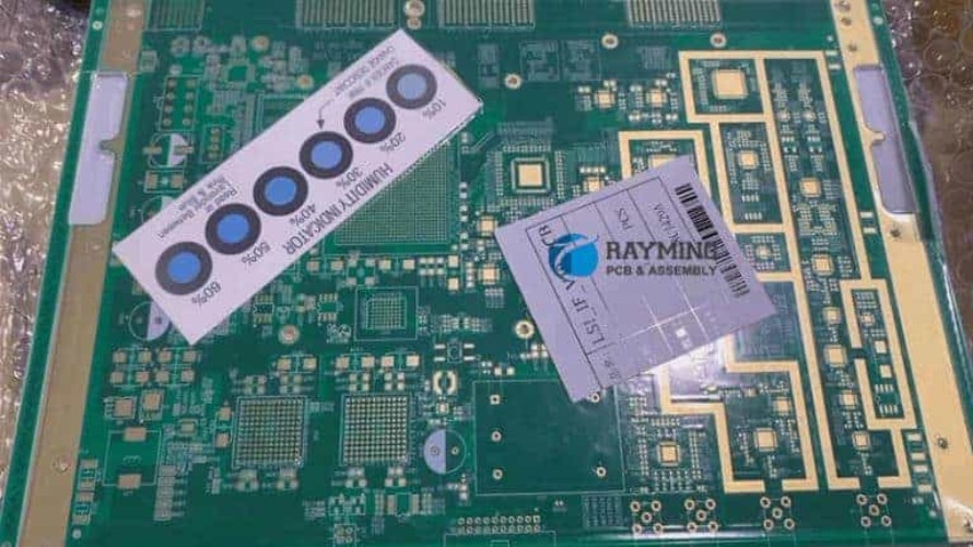
HDI PCB material and fabrication requirements:
- Dielectric materials – Low loss, tight tolerance laminates
- Surface finishes – Thin ENIG or immersion silver recommended
- Laser drilling – For microvias
- Automated optical inspection (AOI) – Detect defects
- Impedance control – Controlled process to match simulated impedances
HDI Reliability Concerns
HDI PCBs present reliability risks due to:
- Thin traces and clearances – More susceptible to shorts and opens
- Microvia reliability – Interface delamination or cracking
- Sensitivity to fabrication defects – Small defects can cause failures
- Via transitions – Impedance mismatches and reflections
Robust design and process control is required to achieve the reliability targets.
Design for Manufacturing
DFM guidelines specific to HDI PCBs:
- Work with manufacturer on stackup design and layer count
- Minimize use of microvias and blind/buried vias if not required
- Maintain minimum trace widths for manufacturability
- Allow for adequate fabrication tolerances
- Perform test coupon runs to qualify line width/space and microvia formation
Summary
HDI PCB technology enables dense interconnection and routing of high pin count ICs. However, they require strict adherence to design guidelines related to trace dimensions, layer stackup, impedance control and reliability. A robust HDI PCB design process including design reviews, simulation and test coupon runs is key to achieving first-pass success.
Frequently Asked Questions
What are the key advantages of HDI PCBs?
The main advantages of HDI PCBs are increased routing density, ability to route high pin count components, improved electrical performance through tight impedance control, and overall miniaturization of electronics.
What are the typical applications for HDI PCBs?
HDI PCBs are used in space constrained and high performance products like smartphones, tablets, base stations, servers, switches, and avionics. Their high density and electrical performance benefits these applications.
What are critical factors impacting HDI PCB reliability?
Critical factors affecting HDI PCB reliability include: trace width and spacing, microvia interface integrity, fabrication process capability and control, handling thin substrates, and matching simulated impedances.
How are microvias formed on HDI PCBs?
The two main methods used to produce microvias in HDI PCBs are laser drilling and photo-process. Laser drilling can drill small diameter holes very accurately while photo-process can create microvias during the patterning steps.
How many HDI layer PCBs are practical today?
With advanced PCB processes, HDI PCBs with 16-24 layers or more are practical today. Even higher layer counts are possible but often have diminishing benefits versus cost and yield impact.
Leave a Reply