Introduction to Layout Design from Schematics
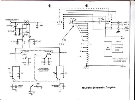
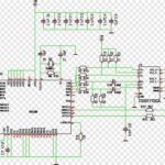
When designing electronic circuits, the schematic captures the electrical connections and components that make up the circuit. However, to physically build the circuit, a layout must be created from the schematic. The layout shows the physical placement of components and routing of traces on a printed circuit board (PCB).
Creating an effective and efficient layout from a schematic requires careful planning and adherence to best practices. This article will provide a comprehensive guide on the process of translating a schematic into a high-quality PCB layout.
Key Steps in Layout Design
The main steps in creating a layout from a schematic are:
- Schematic review and preparation
- Component placement
- Trace routing and copper pour
- Design rule checks (DRC)
- Documentation and manufacturing outputs
We will explore each of these steps in detail.
Schematic Review and Preparation
Importance of Schematic Accuracy
Before beginning the layout process, it is crucial to thoroughly review the schematic for accuracy and completeness. Any errors or omissions in the schematic will carry over to the layout and potentially lead to a non-functional or suboptimal design.
Key aspects to check in the schematic include:
- Component selection and values
- Power supply routing and decoupling
- Signal integrity considerations
- Connector pinouts
- Schematic symbols and footprint associations
Organizing the Schematic for Layout
To facilitate an efficient layout process, it is helpful to organize the schematic in a logical manner. This includes:
- Grouping related components together
- Arranging schematic sheets in a hierarchical structure
- Clearly labeling power nets, ground nets, and important signals
- Adding informative text notes and comments
A well-organized schematic will make it easier to place components and route traces in the layout.
Component Placement
Placement Strategy
Component placement is a critical step in the layout process, as it sets the foundation for routing and largely determines the overall size and shape of the PCB. A good placement strategy should consider:
- Minimizing trace lengths and crossovers
- Optimizing for manufacturability and assembly
- Providing adequate spacing for heat dissipation and mechanical clearance
- Grouping related components together
- Placing connectors and controls for user accessibility
Placement Best Practices
Some best practices for component placement include:
- Place power components close to the power input
- Locate decoupling capacitors close to their associated ICs
- Orient components for easy routing and to minimize trace lengths
- Avoid placing components too close to board edges
- Consider placement of test points and programming headers
| Component Type | Placement Guidelines |
|---|---|
| Power ICs | Close to power input, with room for heatsinking |
| Decoupling caps | As close as possible to IC power pins |
| Connectors | Along board edges for accessibility |
| Crystals/oscillators | Away from noisy components, with short traces |
| Test points | Accessible for probing, away from sensitive signals |
Placing Components in the Layout Tool
Most PCB layout tools provide a component placement mode where you can drag and drop components onto the board outline. It’s generally best to start with the larger, fixed components like connectors and power ICs, then fill in the smaller components.
Many tools also provide an auto-placement feature that can quickly place components based on your schematic connections and design rules. However, auto-placement should be used as a starting point and the results should always be reviewed and tweaked manually.

Trace Routing and Copper Pour
Routing Strategy
Once components are placed, the next step is routing traces to make the electrical connections between them. A good routing strategy should:
- Minimize trace lengths and layer changes
- Provide adequate trace width for current carrying capacity
- Avoid sharp corners and acid traps
- Maintain controlled impedance for high-speed signals
- Separate sensitive signals from noisy ones
Routing Best Practices
Some best practices for trace routing include:
- Route power traces first, using wide traces or copper pours
- Use ground planes to provide shielding and reduce loop areas
- Avoid routing traces under components, especially under SMD pads
- Provide ground stitching vias near connectors to reduce EMI
- Follow manufacturer recommendations for high-speed routing
| Signal Type | Routing Guidelines |
|---|---|
| Power | Wide traces or copper pours, on inner layers when possible |
| Ground | Use ground planes and stitching vias |
| High-speed | Match trace lengths, avoid layer changes, control impedance |
| Analog | Separate from digital signals, use guard rings or traces |
| RF | Follow manufacturer guidelines, avoid sharp bends |
Using Copper Pour
Copper pour, also known as flooding or filling, is the practice of filling unused areas of the board with copper connected to ground or power nets. This has several benefits:
- Reduces EMI by providing shielding
- Improves heat dissipation
- Equalizes Copper Distribution for better etching
- Provides low-impedance paths for return currents
When using copper pour, be sure to set appropriate clearance rules to avoid shorts and leave room for traces. Most layout tools have an automated copper pour feature that will fill in unused areas while obeying clearance rules.
Design Rule Checks (DRC)
What is DRC?
Design rule checking (DRC) is the process of automatically verifying that your layout meets all of the physical and electrical constraints specified by your design rules. This includes checks for:
- Minimum trace width and spacing
- Via size and spacing
- Copper-to-edge clearance
- Silk Screen-to-copper clearance
- Drill-to-copper clearance
- Copper density
- Short circuits and open nets
Running DRC is an essential step before finalizing your layout, as it catches errors that may be difficult to spot visually.
Setting Up DRC Rules
To run DRC, you first need to set up your design rules in your layout tool. This usually involves specifying values for parameters like:
- Minimum trace width
- Minimum trace spacing
- Minimum via size
- Minimum via spacing
- Minimum drill size
Your PCB manufacturer will provide recommended values for these parameters based on their capabilities. You can also specify different rules for different net classes, such as wider spacing for high-voltage nets.
Running and Interpreting DRC Results
Once your design rules are set up, you can run DRC on your layout. The tool will check your layout against the rules and report any violations.
Violations are typically displayed as markers on the layout, and clicking a marker will bring up details about the specific rule that was violated. It’s important to review and address all DRC violations before considering your layout complete.
Some common DRC violations and their fixes:
| Violation | Typical Fix |
|---|---|
| Trace too close to pad | Move trace or adjust pad size |
| Trace too close to edge | Move trace inward or increase board size |
| Via too small | Increase via size or change to a larger drill |
| Copper area too small | Enlarge copper pour or add thermally-relieved pads |
| Silk overlap on pad | Move silkscreen or adjust pad size |
Documentation and Manufacturing Outputs
Generating Fabrication Drawings
Once your layout is complete and has passed DRC, you need to generate fabrication files to send to your PCB manufacturer. These typically include:
- Gerber files for each copper layer, solder mask, and silk screen
- Drill files specifying hole locations and sizes
- Centroid file for automated assembly
- Bill of Materials (BOM) listing all components
Your layout tool will have a feature to export these files in the formats required by your manufacturer.
Creating Assembly Drawings
In addition to fabrication files, it’s often helpful to create assembly drawings to aid in PCB Assembly. These drawings show:
- Component locations and orientations
- Reference designators
- Any special assembly instructions
Assembly drawings can be created in your layout tool or in a separate drawing program.
Reviewing Manufacturability
Before sending your files off for manufacturing, it’s a good idea to do a final review for manufacturability. This includes checking:
- Minimum hole size and spacing
- Soldermask and silkscreen clearances
- Copper balancing and density
- Any special requirements like impedance control or surface finish
Your PCB manufacturer can provide guidance on their capabilities and any necessary adjustments to your design.
FAQ
What is the difference between a schematic and a layout?
A schematic is a symbolic representation of the electrical connections in a circuit, while a layout is the physical implementation of that circuit on a PCB. The schematic shows how components are connected electrically, while the layout shows where those components are physically placed and how they are interconnected with copper traces.
Can I automate the process of creating a layout from a schematic?
To some extent, yes. Many PCB layout tools have auto-placement and auto-routing features that can automatically place components and route traces based on your schematic and design rules. However, these automated results should always be reviewed and fine-tuned manually, as they may not take into account all of the nuances of your specific design.
What are some common mistakes to avoid when creating a PCB layout?
Some common PCB layout mistakes include:
- Not properly reviewing the schematic before starting layout
- Placing components too close together or too close to board edges
- Not providing adequate trace width for current carrying capacity
- Routing high-speed signals without regard for impedance control
- Not running design rule checks (DRC) before finalizing the layout
How do I choose the right trace width for my PCB layout?
Trace width is determined by the amount of current the trace needs to carry, as well as any impedance control requirements. Wider traces can carry more current and have lower resistance, but they also take up more space. Your PCB manufacturer can provide recommendations for minimum trace width based on your Copper Weight and current requirements. For high-speed signals, trace width is also determined by the desired characteristic impedance, which can be calculated based on your PCB Stackup and material properties.
What is the purpose of copper pour in a PCB layout?
Copper pour, also known as copper fill or flooding, serves several purposes in a PCB layout:
- It provides low-impedance return paths for currents, which can reduce EMI and improve signal integrity.
- It helps to evenly distribute copper on the board, which can prevent warping during manufacturing.
- It can act as a heat sink to dissipate heat from power components.
- It can provide shielding to sensitive signals.
Copper pour is typically connected to ground, but can also be connected to power nets in some cases. When using copper pour, be sure to set appropriate clearance rules to avoid inadvertent shorts to traces or components.
I hope this article provides a helpful overview of the process of creating a PCB layout from a schematic. Remember, the key to a successful layout is careful planning, attention to detail, and adherence to best practices and design rules. Happy layouting!
Leave a Reply