Introduction to COB and SMD LED Technology
Light-emitting diode (LED) technology has revolutionized the lighting industry, offering energy-efficient and long-lasting solutions for various applications. Two popular types of LED packaging are Chip-on-Board (COB) and Surface-Mount Device (SMD). In this comprehensive article, we will explore the manufacturing and assembly processes of COB and SMD LED printed circuit boards (PCBs) from start to finish.
What are COB and SMD LEDs?
COB LEDs are created by directly mounting multiple LED chips onto a substrate, which is then covered with a phosphor layer to produce the desired color temperature. This packaging method allows for high-density LED arrays, resulting in improved light output and thermal management.
SMD LEDs, on the other hand, are individual LED packages that are soldered onto a PCB. They are smaller in size compared to COB LEDs and offer greater flexibility in terms of design and layout.
PCB Manufacturing Process for COB and SMD LEDs
The manufacturing process for COB and SMD LED PCBs involves several key steps:
1. PCB Design and Layout
The first step in the manufacturing process is to design the PCB layout using specialized software such as Altium Designer or KiCad. The layout must take into account the specific requirements of the COB or SMD LEDs, including thermal management, electrical characteristics, and optical performance.
2. PCB Fabrication
Once the PCB design is finalized, the fabrication process begins. This typically involves the following steps:
- Substrate preparation: The PCB substrate, usually made of FR-4 or aluminum, is cleaned and treated to ensure proper adhesion of the copper layer.
- Copper lamination: A thin layer of copper is laminated onto the substrate using heat and pressure.
- Photoresist application: A photoresist layer is applied to the copper surface and exposed to UV light through a photomask, which contains the PCB layout pattern.
- Etching: The exposed copper is etched away using a chemical solution, leaving behind the desired circuit pattern.
- Soldermask and silkscreen: A soldermask layer is applied to protect the copper traces, and a silkscreen layer is added for component labeling and identification.
3. PCB Assembly
After the PCB fabrication is complete, the assembly process begins. For COB LEDs, this involves the following steps:
- Die bonding: The LED chips are bonded to the PCB substrate using a conductive adhesive or Eutectic Soldering process.
- Wire bonding: Thin gold or aluminum wires are used to establish electrical connections between the LED chips and the PCB.
- Phosphor coating: A phosphor layer is applied over the LED chips to convert the blue light emitted by the chips into the desired color temperature.
- Encapsulation: A silicone or epoxy encapsulant is used to protect the LED chips and wire bonds from environmental factors.
For SMD LEDs, the assembly process is slightly different:
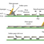
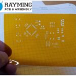
- Solder paste application: Solder paste is applied to the PCB pads using a stencil or syringe.
- Pick and place: An automated pick-and-place machine is used to place the SMD LEDs onto the PCB pads with high precision.
- Reflow soldering: The PCB is passed through a reflow oven, which melts the solder paste and establishes electrical and mechanical connections between the SMD LEDs and the PCB.
Thermal Management Considerations
One of the critical aspects of COB and SMD LED PCB manufacturing is thermal management. LEDs generate a significant amount of heat during operation, which can negatively impact their performance and lifespan if not properly dissipated.
For COB LEDs, thermal management is typically achieved through the use of Metal-Core PCBs (MCPCBs) or aluminum substrates. These materials have high thermal conductivity, allowing for efficient heat transfer from the LED chips to the PCB and ultimately to the heatsink.
SMD LEDs rely on thermal vias and copper pours on the PCB to conduct heat away from the LED packages. The PCB layout must be designed to optimize thermal dissipation, with adequate spacing between LEDs and sufficient copper coverage.

Quality Control and Testing
To ensure the quality and reliability of COB and SMD LED PCBs, several testing and inspection procedures are carried out at various stages of the manufacturing process:
- Visual inspection: The PCBs are visually inspected for any defects, such as scratches, dents, or discoloration.
- Automated optical inspection (AOI): An AOI machine is used to detect any missing or misaligned components, solder bridging, or other assembly defects.
- Electrical testing: The PCBs are subjected to electrical tests to verify their functionality and ensure that they meet the specified performance parameters.
- Burn-in testing: The assembled PCBs are operated at elevated temperatures for an extended period to identify any early failures or performance degradation.
- Chromaticity and luminosity testing: The color temperature and light output of the COB or SMD LEDs are measured to ensure consistency and adherence to the specified requirements.
Applications of COB and SMD LED PCBs
COB and SMD LED PCBs find applications in a wide range of industries and products, including:
- General lighting: Indoor and outdoor lighting fixtures, such as downlights, spotlights, and floodlights.
- Automotive lighting: Headlights, taillights, and interior lighting in vehicles.
- Display backlighting: Backlighting for LCD and OLED displays in televisions, monitors, and mobile devices.
- Horticulture lighting: Grow lights for indoor farming and greenhouse applications.
- Medical devices: Surgical lighting, endoscopy, and dental equipment.
Future Trends in COB and SMD LED PCB Manufacturing
As LED technology continues to evolve, several trends are expected to shape the future of COB and SMD LED PCB manufacturing:
- Miniaturization: The development of smaller LED packages and higher-density PCB layouts will enable more compact and efficient lighting solutions.
- Flexible and stretchable PCBs: The use of flexible and stretchable PCB materials will allow for the integration of LEDs into wearable devices and unconventional form factors.
- Smart lighting: The incorporation of wireless connectivity and sensors into LED PCBs will enable the development of smart lighting systems with advanced features such as color tuning, dimming, and occupancy sensing.
- Sustainable manufacturing: There will be an increased focus on environmentally friendly materials and processes in LED PCB manufacturing, such as the use of lead-free solders and recyclable substrates.
Conclusion
COB and SMD LED PCB manufacturing is a complex process that involves multiple stages, from PCB design and fabrication to assembly and testing. By understanding the key aspects of this process, including thermal management, quality control, and application-specific requirements, manufacturers can produce high-quality and reliable LED lighting solutions. As technology advances, the future of COB and SMD LED PCB manufacturing looks bright, with exciting new possibilities on the horizon.
Frequently Asked Questions (FAQ)
1. What is the difference between COB and SMD LEDs?
COB LEDs are created by mounting multiple LED chips directly onto a substrate and covering them with a phosphor layer, while SMD LEDs are individual LED packages that are soldered onto a PCB.
2. What materials are used for COB LED substrates?
COB LED substrates are typically made of metal-core PCBs (MCPCBs) or aluminum, which offer high thermal conductivity for efficient heat dissipation.
3. How are SMD LEDs attached to the PCB?
SMD LEDs are attached to the PCB using a reflow soldering process. Solder paste is applied to the PCB pads, and the SMD LEDs are placed onto the pads using a pick-and-place machine. The PCB is then passed through a reflow oven to melt the solder and establish electrical and mechanical connections.
4. What are the advantages of using COB LEDs?
COB LEDs offer several advantages, including high light output, excellent thermal management, and a compact form factor. They are well-suited for applications that require high-intensity illumination, such as spotlights and floodlights.
5. What testing procedures are used to ensure the quality of COB and SMD LED PCBs?
COB and SMD LED PCBs undergo various testing procedures, including visual inspection, automated optical inspection (AOI), electrical testing, burn-in testing, and chromaticity and luminosity testing. These tests help ensure the quality, reliability, and performance of the LED lighting solutions.
| Aspect | COB LEDs | SMD LEDs |
|---|---|---|
| Packaging | Multiple LED chips mounted directly on a substrate | Individual LED packages soldered onto a PCB |
| Substrate Materials | Metal-core PCBs (MCPCBs) or aluminum | Standard PCB materials (e.g., FR-4) |
| Thermal Management | Excellent thermal conductivity due to substrate materials | Relies on thermal vias and copper pours on the PCB |
| Light Output | High-intensity illumination | Varies based on the number and type of SMD LEDs used |
| Application Examples | Spotlights, floodlights, high-bay lighting | Backlighting, indicator lights, automotive lighting |


Leave a Reply