PCB Blog
-
Read more: PCB Soldering-15 Common PCB Soldering Problems to Avoid
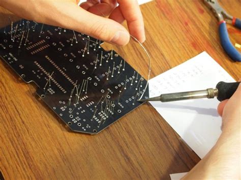
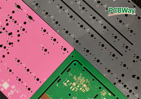
Insufficient Wetting Insufficient wetting occurs when the solder does not flow properly onto the surface of the PCB or the component leads. This can result in a weak or incomplete solder joint, which can lead to electrical failures. Causes of Insufficient Wetting Contaminated or oxidized surfaces Incorrect solder temperature Insufficient flux Incorrect solder alloy Solutions…
-
What are Tented Vias?
Posted by
–
 Read more: What are Tented Vias?
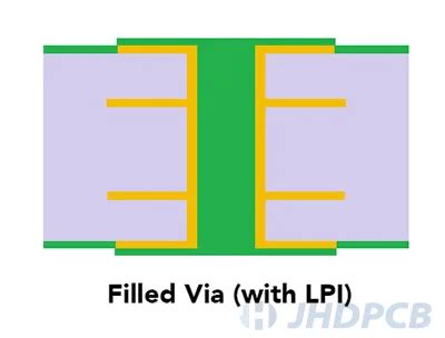
Introduction to Tented Vias Tented vias are a type of via structure used in printed circuit board (PCB) design and manufacturing. Vias are small holes drilled through a PCB that allow electrical connections between different layers of the board. In the case of tented vias, these holes are covered or “tented” with solder mask on…
-
How Can You Repair the Solder Mask on a PCB?
Posted by
–
 Read more: How Can You Repair the Solder Mask on a PCB?
Understanding Solder Mask and Its Importance Solder mask, also known as solder resist or solder stop, is a protective layer applied to the copper traces of a printed circuit board (PCB). This layer serves several crucial functions, including: Preventing accidental short circuits by isolating the copper traces Protecting the copper from oxidation and corrosion Providing…
-
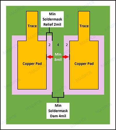
 Read more: Soldermask Expansion is the value applied to SMD pads
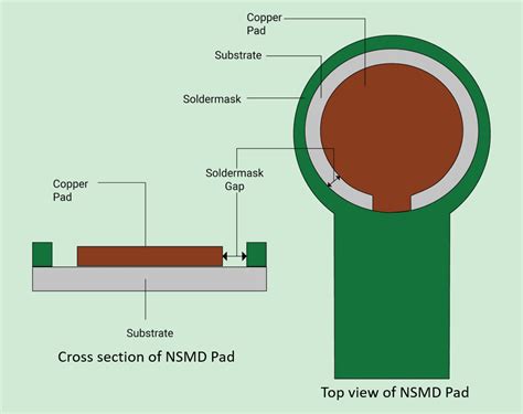
What is Soldermask Expansion? Soldermask expansion, also known as solder resist expansion or solder mask pullback, refers to the amount that the soldermask pulls back from the edges of the copper pads on a printed circuit board (PCB). It is an important design parameter in PCB manufacturing that affects the solderability, reliability, and manufacturability of…
-
What Are The Functions of Solder Mask in PCB?
Posted by
–
 Read more: What Are The Functions of Solder Mask in PCB?
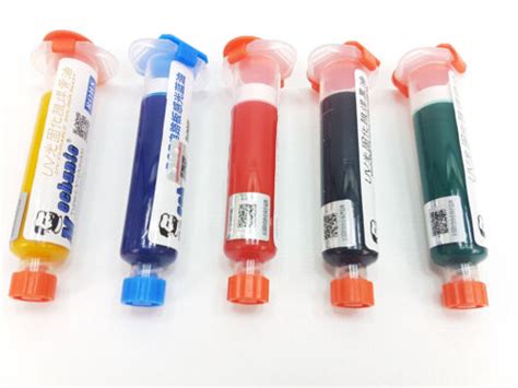
What is Solder Mask? Solder mask, also known as solder resist or solder stop, is a thin layer of polymer applied to the surface of a PCB. It is typically green in color but can also be found in other colors such as red, blue, or black. The primary purpose of solder mask is to…
-
 Read more: The common problems and solutions of PCB soldermask
What is PCB Soldermask? PCB soldermask, also known as solder resist or solder mask, is a thin layer of polymer that is applied to the copper traces of a printed circuit board (PCB). Its primary purpose is to protect the copper traces from oxidation, prevent solder bridges from forming between closely spaced pads, and provide…
-
What s the impact of the soldermask thickness?
Posted by
–
 Read more: What s the impact of the soldermask thickness?
Why is Soldermask Thickness Important? The thickness of the soldermask layer is a critical factor in PCB design and manufacturing for several reasons: Insulation: Soldermask acts as an insulating layer, preventing unwanted electrical connections between copper traces. The thickness of the soldermask directly affects its insulating properties. Protection: Soldermask protects the copper traces from oxidation,…
-
Blue Soldermask is Easier to Distinguish
Posted by
–
 Read more: Blue Soldermask is Easier to Distinguish
What is Soldermask and Why is Blue Soldermask Popular? Soldermask, also known as solder resist or solder mask, is a thin lacquer-like layer of polymer applied to the copper traces of a printed circuit board (PCB). Its primary purpose is to prevent solder from bridging between conductors, thereby preventing short circuits. Soldermask also provides protection…
-
How to Test PCB Soldermask?
Posted by
–
 Read more: How to Test PCB Soldermask?
What is PCB Soldermask? PCB soldermask, also known as solder resist or solder mask, is a protective layer applied to the copper traces of a printed circuit board (PCB) to prevent solder from bridging between conductors during the soldering process. It also provides insulation and protection against oxidation and environmental contaminants. Soldermask is typically a…
-
4 Main Types of PCB Solder Mask
Posted by
–
 Read more: 4 Main Types of PCB Solder Mask
What is PCB Solder Mask? PCB solder mask, also known as solder resist or solder stop mask, is a thin lacquer-like layer of polymer applied to the copper traces of a printed circuit board (PCB). Its primary purpose is to prevent solder bridges from forming between closely spaced solder pads during the soldering process. Additionally,…


