PCB Blog
-
 Read more: Any Layer HDI PCB: A Revolution in High-Density Interconnect PCBs
Introduction High-density interconnect (HDI) PCBs have transformed the world of electronics by enabling much higher component densities and circuit complexity than previously possible. Traditional HDI PCBs use microvias to interconnect layers and allow traces and spaces under 6 mils. However, these PCBs typically have a limitation: the microvias can only […]
-
The Advantages of Anylayer PCBs
Posted by
–
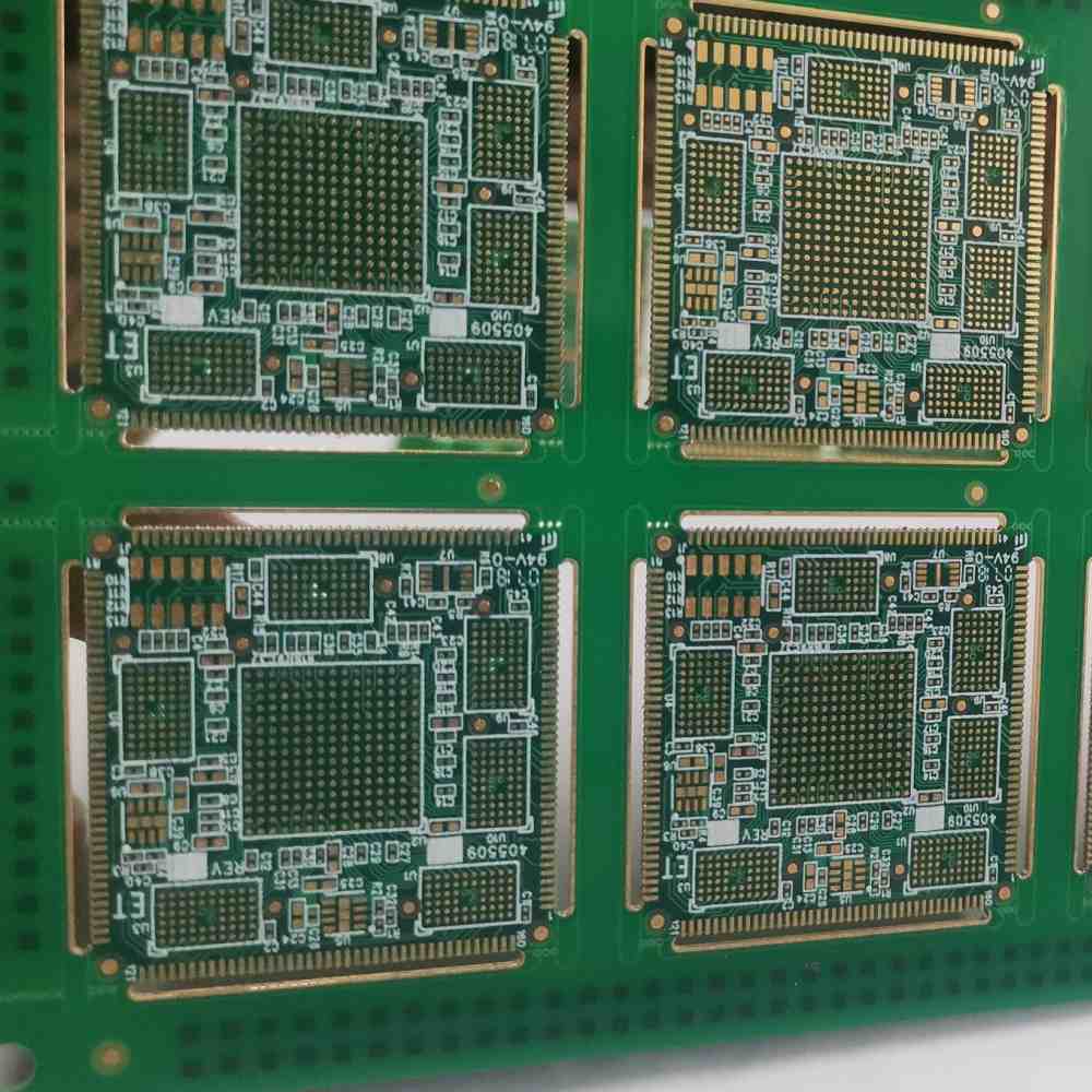 Read more: The Advantages of Anylayer PCBs
Introduction Printed circuit boards (PCBs) are essential components in almost all modern electronics. As electronic devices become more complex and compact, there is an increasing need for PCBs that can accommodate more intricate circuit designs. This is where anylayer PCBs come in. Anylayer PCBs allow traces and routing on any […]
-
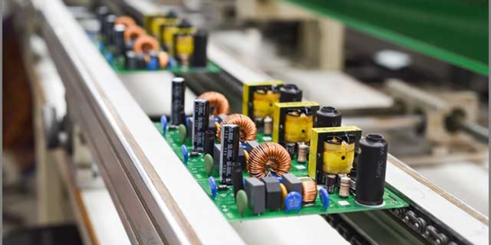 Read more: Automated Circuit Board Assembly: The Future of Electronics Manufacturing
Introduction to Automated Circuit Board Assembly Printed circuit boards (PCBs) are essential components in nearly all modern electronics. They provide the foundation on which microchips, resistors, capacitors and other components are mounted and connected to create functional electronic devices. The assembly of PCBs has traditionally been a manual process requiring […]
-
Bare Printed Circuit Board Manufacturing
Posted by
–
 Read more: Bare Printed Circuit Board Manufacturing
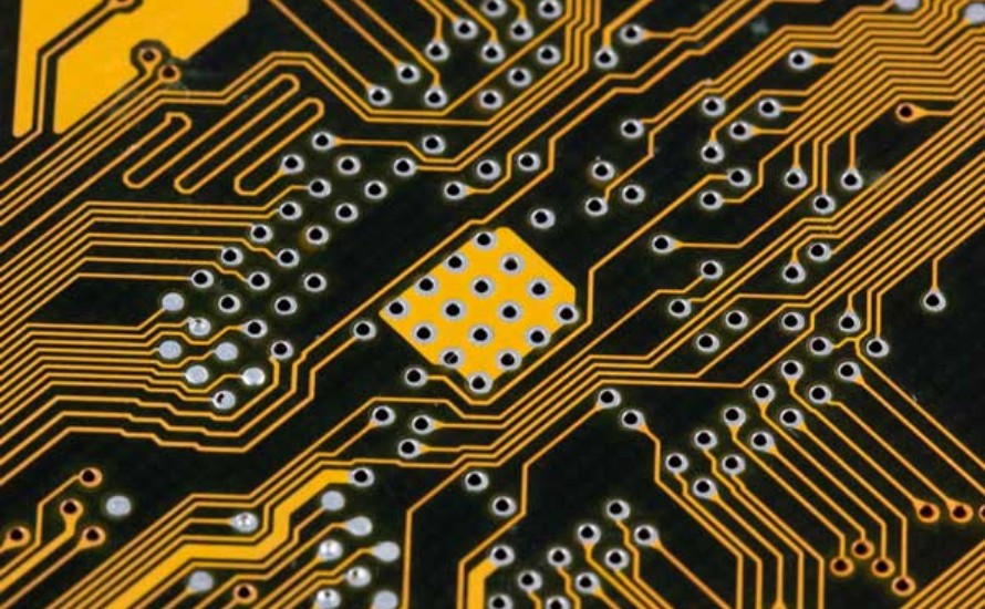
Introduction to Bare PCBs A printed circuit board (PCB) forms the backbone of any electronic device. It provides the mechanical structure to mount and interconnect electronic components using conductive copper traces etched from copper sheets laminated onto a non-conductive substrate. Bare PCBs contain only the bare minimum – a laminated […]
-
Blind and Buried Vias in PCB Design
Posted by
–
 Read more: Blind and Buried Vias in PCB Design
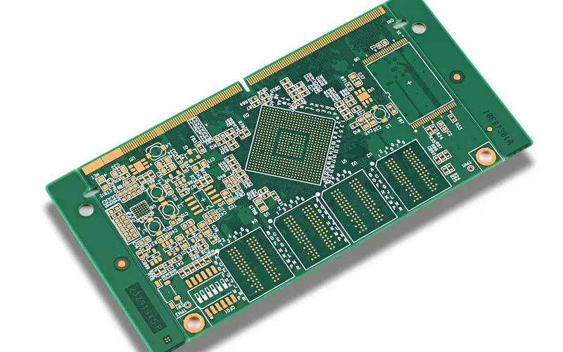
Introduction In printed circuit board (PCB) design, vias are plated through holes that provide electrical connections between layers in the board. Vias come in several types, including blind, buried, and through-hole vias. Blind and buried vias are important for high-density interconnects in multilayer PCBs. In this article, we will discuss […]
-
 Read more: Blind Buried Vias: A Critical Interconnect Technology for High-Density PCBs
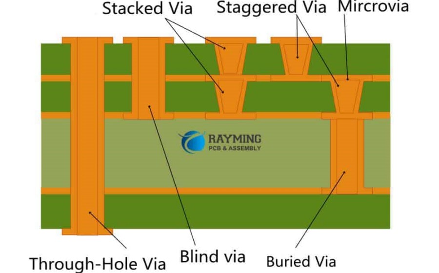
Introduction Printed circuit boards (PCBs) are essential components of nearly all modern electronic devices, serving to mechanically support and electrically connect electronic components. As electronic products continue to be designed smaller and with greater functionality, PCBs have evolved to accommodate more complex circuitry and components in increasingly compact spaces. This […]
-
Blind Hole PCBs: A Complete Guide
Posted by
–
 Read more: Blind Hole PCBs: A Complete Guide
Blind holes, also known as buried vias, are an essential component in printed circuit board (PCB) design. As electronics become more complex and compact, the use of blind vias helps connect different layers efficiently without using up valuable surface space. This article will provide a comprehensive overview of blind hole […]
-
 Read more: The Blind Via Manufacturing Process for Printed Circuit Boards
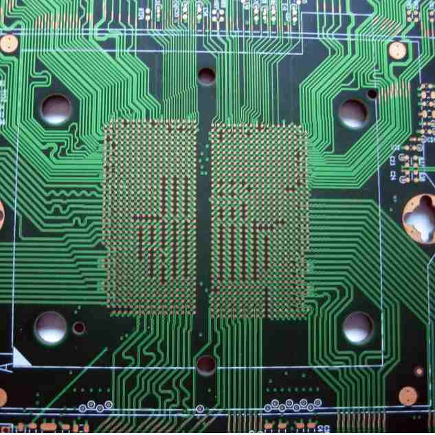
Introduction Printed circuit boards (PCBs) are essential components in virtually all modern electronics. They provide the physical structure and electrical connections between components in an electronic device. A key part of PCB design and manufacturing is creating vias – holes that connect different layers of copper traces in the board. […]
-
Blind Via Design in Altium
Posted by
–
 Read more: Blind Via Design in Altium
Introduction Blind vias are an essential component in many printed circuit board (PCB) designs today. A blind via is a hole that connects different layers of a PCB without going all the way through the entire board. Blind vias allow connections between internal layers of a multilayer board while avoiding […]
-
 Read more: Blind Via and Buried Via: A Comparison of PCB Vias
Printed circuit boards (PCBs) use vias to create connections between different layers of the board. Vias come in several types, with two of the most common being blind vias and buried vias. Understanding the differences between these via types and when to use each one is important for PCB designers. […]
