PCB Blog
-
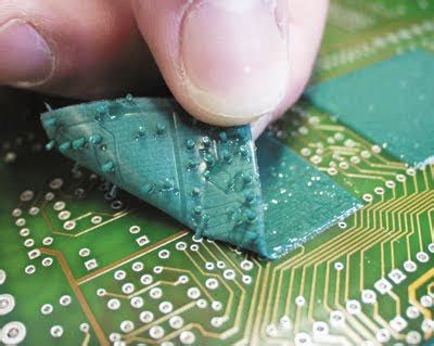
How is solder mask applied on PCB
Posted by
–
Read more: How is solder mask applied on PCBWhat is Solder Mask? Solder mask, also known as solder resist or solder stop, is a protective coating applied to the copper traces of a printed circuit board (PCB) to prevent accidental short circuits and to protect the copper from oxidation. It is a thin, permanent layer of polymer that is applied to the PCB…
-
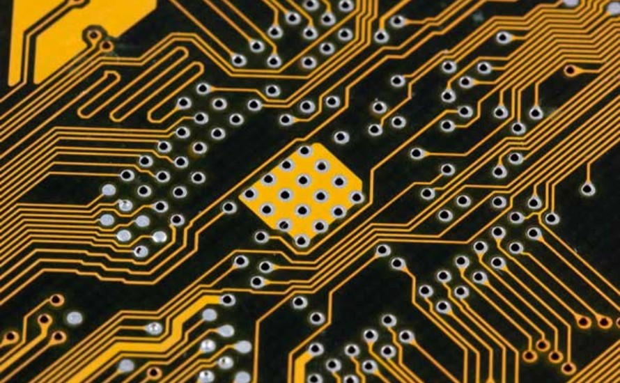
HDI PCB Industries and Applications
Posted by
–
 Read more: HDI PCB Industries and Applications
Introduction to HDI PCBs HDI (High Density Interconnect) PCBs refer to printed circuit boards with a higher wiring density than traditional PCBs. They allow trace spacings and wire widths under 100 microns, whereas standard PCBs only allow minimum spacings of around 150 – 250 microns. HDI PCBs provide the following benefits: Some key technologies used…
-
Types of Vias in HDI PCB Routing
Posted by
–
 Read more: Types of Vias in HDI PCB Routing
Introduction High density interconnect (HDI) printed circuit boards (PCBs) have emerged as an essential technology for many advanced electronics designs today. HDI PCBs allow routing of traces with extremely fine lines and spaces, enabling higher component densities and more compact layouts. One of the key enablers of HDI PCBs are microvias – small vias with…
-
Read more: Design Your Feature Size to Satisfy HDI DFM Requirements
Introduction As modern electronics continue to pack more functionality into smaller packages, high density interconnect (HDI) printed circuit boards (PCBs) have become essential for many applications. HDI PCBs allow routing of traces between very closely spaced components, enabling miniaturized and lightweight products. However, the design rules for HDI are much tighter than for conventional PCBs.…
-
 Read more: Overview of HDI PCB Board Design and Manufacturing Processes
Introduction to High Density Interconnect (HDI) PCBs High density interconnect (HDI) PCBs are printed circuit boards with a higher wiring density than conventional PCBs. They enable the miniaturization of electronic devices by accommodating a high number of interconnects in a small surface area. Some key characteristics of HDI PCBs are: The main benefits of HDI…
-
 Read more: What’s Different About HDI PCB Board Design and Manufacturing?
Introduction HDI (High Density Interconnect) PCBs are printed circuit boards with higher wiring densities than conventional PCBs. HDI technology allows traces and spaces between traces to be reduced to smaller dimensions, allowing more signal routing in the same area. This enables products to be made smaller and more compact with increased functionality. HDI PCBs require…
-
 Read more: Design Guidelines for High Density Interconnect (HDI) PCBs
Introduction High density interconnect (HDI) PCBs contain traces and spaces that are considerably finer than those found on conventional PCBs. HDI PCBs enable higher component densities and more interconnect on the same PCB area. They are essential for the miniaturization and performance requirements of modern electronics. However, designing HDI PCBs requires following strict layout guidelines…
-
 Read more: ELIC (Every Layer Interconnection): Most Complex HDI
Introduction High density interconnect (HDI) printed circuit boards (PCBs) have become increasingly popular in recent years due to the growing demand for smaller and more complex electronic devices. As components shrink in size and increase in number, PCB designers must find ways to accommodate all the necessary interconnects in a limited space. This has led…
-
HDI PCB (2+N+2): Moderate Complex HDI
Posted by
–
 Read more: HDI PCB (2+N+2): Moderate Complex HDI
Introduction High density interconnect (HDI) PCBs have become increasingly common in consumer electronics and other electronic devices where space is at a premium. HDI allows for denser routing between components, enabling smaller and more compact PCB designs. One configuration of HDI PCBs is known as 2+N+2, referring to the number of conductive layers. This article…
-
HDI PCB (1+N+1): Simplest HDI
Posted by
–
Read more: HDI PCB (1+N+1): Simplest HDIIntroduction High-density interconnect (HDI) PCBs have become increasingly popular in recent years due to the continued miniaturization of electronics. HDI allows for tighter routing spaces, more signal layers, finer lines and spaces, microvias, and other features not possible on conventional PCBs. The 1+N+1 HDI stackup is one of the simplest HDI configurations, making it an…


