PCB Blog
-
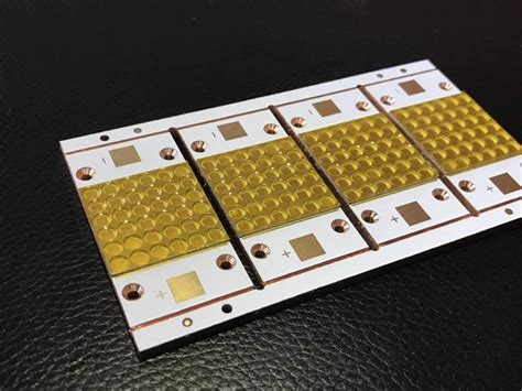
What is the core of a PCB?
Posted by
–
Read more: What is the core of a PCB?What is a Core PCB? A core PCB, also known as the substrate or base material, is the insulating layer that forms the backbone of a printed circuit board. It is typically made of a dielectric material, such as FR-4 (a glass-reinforced epoxy laminate), which provides electrical insulation and mechanical […]
-
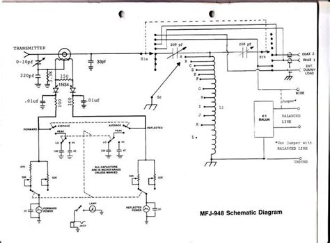
Creating the Layout from your Schematic
Posted by
–
 Read more: Creating the Layout from your Schematic
Introduction to Layout Design from Schematics When designing electronic circuits, the schematic captures the electrical connections and components that make up the circuit. However, to physically build the circuit, a layout must be created from the schematic. The layout shows the physical placement of components and routing of traces on […]
-
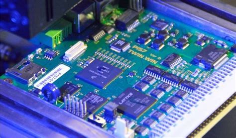
PCBA Visualizer – User Guide – BOM Editor
Posted by
–
 Read more: PCBA Visualizer – User Guide – BOM Editor
Introduction to PCBA Visualizer PCBA Visualizer is a powerful tool designed to streamline the process of visualizing and editing Bill of Materials (BOM) for Printed Circuit Board Assemblies (PCBAs). This user-friendly software provides a comprehensive set of features that enable engineers, designers, and manufacturers to efficiently manage and optimize their […]
-
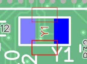
PCBA Visualizer – User Guide – CPL Editor
Posted by
–
 Read more: PCBA Visualizer – User Guide – CPL Editor
Introduction to PCBA Visualizer PCBA Visualizer is a powerful tool for visualizing and analyzing printed circuit board assemblies (PCBAs). It allows engineers, designers, and manufacturers to view and interact with 3D models of PCBAs, helping to streamline the design and manufacturing process. With PCBA Visualizer, users can: View and manipulate […]
-
RF pool – insights and details
Posted by
–
 Read more: RF pool – insights and details
Introduction to RF pool and its importance An RF (radio frequency) pool is a critical component in modern wireless communication systems. It refers to a shared collection of radio frequency resources that are dynamically allocated to different users and devices based on their requirements. The efficient management and utilization of […]
-
IOT Solutions World Congress 2024
Posted by
–
 Read more: IOT Solutions World Congress 2024
What to Expect at IoTSWC 2024 IoTSWC 2024 promises to be bigger and better than ever, with an expanded exhibition area, a comprehensive conference program, and numerous networking opportunities. Attendees can expect to: Discover cutting-edge IoT Solutions and technologies Learn from industry experts through keynote speeches, panel discussions, and workshops […]
-
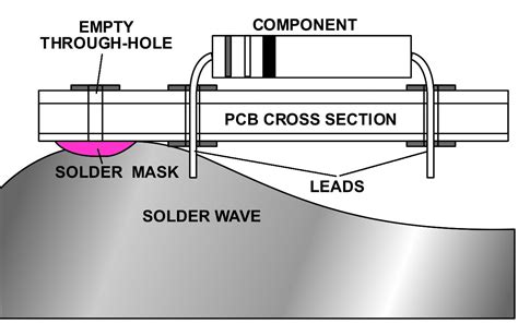 Read more: Tips & Tricks: Avoiding Solder Escape/Wick during Reflow
What is Solder Escape? Solder escape, also known as solder wicking, is a common issue in Electronic Assembly where molten solder flows or “wicks” away from the intended joint, along the component lead or PCB trace. This can result in insufficient solder at the joint, leading to poor electrical connections, […]
-
How do you prevent Solder Escape/Wick?
Posted by
–
 Read more: How do you prevent Solder Escape/Wick?
Understanding Solder Escape What is Solder Escape? Solder escape, also known as Solder Wicking, is a phenomenon that occurs during the soldering process when molten solder is unintentionally drawn away from the intended connection point. Instead of forming a strong and reliable solder joint, the solder travels along component leads, […]
-
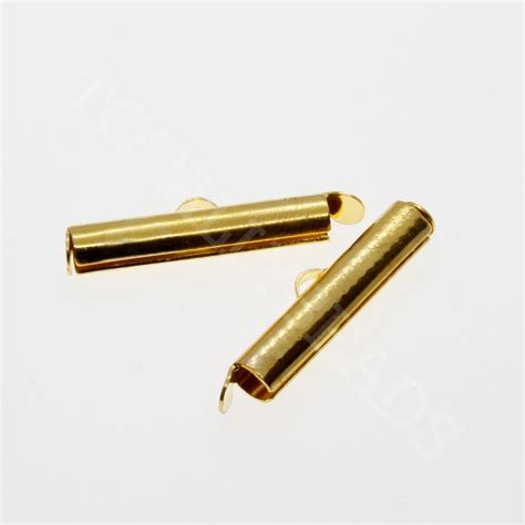
Edge Connectors with Gold Surface
Posted by
–
 Read more: Edge Connectors with Gold Surface
Introduction to Gold-Plated Edge Connectors Gold-plated edge connectors are a type of electrical connector commonly used in various electronic devices, such as computers, telecommunications equipment, and industrial machinery. These connectors are designed to provide a reliable and efficient means of connecting printed circuit boards (PCBs) to other components or systems. […]
-
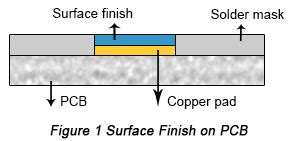
Selecting the Right Surface Finish for Your PCB
Posted by
–
 Read more: Selecting the Right Surface Finish for Your PCB
What is a PCB Surface Finish? A PCB surface finish is a coating applied to the exposed copper traces and pads on a printed circuit board. Its primary purpose is to protect the copper from oxidation and corrosion, which can occur due to exposure to air, moisture, and other environmental […]


