PCB Blog
-
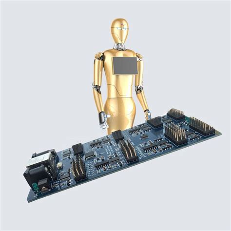
The PCB’s in our Robots
Posted by
–
Read more: The PCB’s in our RobotsWhat are PCBs and Why are They Essential in Robotics? PCBs are thin, flat boards made of insulating material, typically fiberglass or plastic, with conductive copper tracks etched onto their surface. These boards serve as the foundation for mounting and interconnecting electronic components such as microcontrollers, sensors, actuators, and power modules. PCBs provide a compact…
-
 Read more: Some PCB Design Guidelines You Need to Know An Advise From a PCB Engineer
Understanding the Basics of PCB Design Before diving into the specifIC Guidelines, it’s essential to understand the basics of PCB design. A PCB is a flat board made of insulating material, such as fiberglass or plastic, with conductive copper traces etched onto its surface. These traces connect various electronic components, such as resistors, capacitors, and…
-
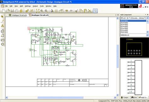
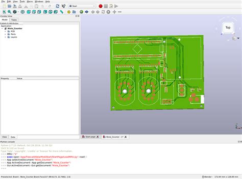
DesignSpark PCB Design Software for Windows PCs
Posted by
–
 Read more: DesignSpark PCB Design Software for Windows PCs
Introduction to DesignSpark PCB DesignSpark PCB is a powerful yet easy-to-use printed circuit board (PCB) design software for Windows computers. Developed by RS Components, DesignSpark PCB enables engineers, hobbyists, and students to quickly design professional quality PCBs for prototyping or small production runs. Some key features of DesignSpark PCB include: – Schematic capture and PCB…
-
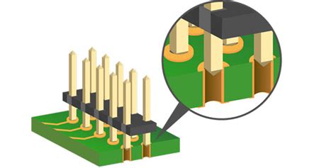
 Read more: Component Placement onto the Printed Circuit Board
Introduction to PCB Component Placement Printed Circuit Board (PCB) component placement is a crucial step in the PCB Assembly process. It involves strategically positioning electronic components on the board to optimize performance, minimize interference, and facilitate efficient manufacturing. Proper component placement ensures the reliability, functionality, and manufacturability of the final product. In this article, we…
-
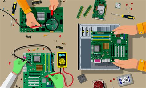
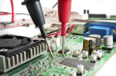
Common PCB PCBA Testing Techniques
Posted by
–
 Read more: Common PCB PCBA Testing Techniques
Introduction to PCB Testing Printed Circuit Boards (PCBs) and Printed Circuit Board Assemblies (PCBAs) are essential components in modern electronic devices. To ensure the reliability and functionality of these components, various testing techniques are employed throughout the manufacturing process. In this article, we will explore the common PCB and PCBA Testing techniques used in the…
-
Tips & Tricks – Why Do Components Tombstone
Posted by
–
 Read more: Tips & Tricks – Why Do Components Tombstone
What Does it Mean When Components Tombstone? “Tombstoning” is a phenomenon that can occur with surface mount electronic components during the Reflow Soldering process in PCB Assembly. When a component tombstones, one end lifts up vertically from the solder pad while the other end remains attached. The component ends up standing on end like a…
-
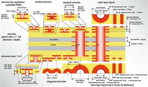
 Read more: PCB Classification – pattern class and drill class
Introduction to PCB Classification Printed Circuit Boards (PCBs) are essential components in modern electronics, providing a platform for interconnecting electronic components and facilitating the flow of electrical signals. To ensure the proper functioning and reliability of PCBs, it is crucial to classify them based on various criteria. Two key aspects of PCB classification are pattern…
-
What is the typical tolerance for PCB?
Posted by
–
 Read more: What is the typical tolerance for PCB?
Understanding PCB tolerance PCB tolerance is a critical aspect of PCB design and manufacturing. It defines the acceptable range of deviation from the ideal or specified dimensions and measurements. These tolerances are necessary to ensure that the PCB fits properly within the designated space in the electronic device, connects correctly with other components, and functions…
-
PCB Visualizer very much appreciated
Posted by
–
 Read more: PCB Visualizer very much appreciated
What is a PCB Visualizer? A PCB Visualizer is a powerful software tool that enables engineers and designers to create, visualize, and analyze printed circuit board (PCB) designs in a virtual environment. This innovative technology has revolutionized the way PCBs are designed and manufactured, streamlining the process and reducing the risk of errors. Key Features…
-
Understanding Manufacturing Tolerances on a PCB – Track Width and Isolation Gap Tolerances
Posted by
–
 Read more: Understanding Manufacturing Tolerances on a PCB – Track Width and Isolation Gap Tolerances
What are PCB Tolerances? PCB tolerances refer to the acceptable variations in the dimensions and properties of a PCB during the manufacturing process. These tolerances are necessary because it is virtually impossible to manufacture a PCB with exact dimensions and specifications every single time. Tolerances allow for slight deviations from the ideal measurements while still…


