Introduction to Buried Vias
Buried vias are a type of via used in printed circuit boards (PCBs) that connect different layers internally in the board without being exposed on the outer surfaces. Unlike traditional through-hole vias that penetrate the entire PCB, buried vias are contained between layers inside the board.
Buried vias provide several benefits compared to through-hole vias:
- More routing space on outer layers since vias don’t break out on surface
- Allows higher component density by reducing space used by vias
- Improved signal integrity from reduced stub effects of via barrels
- Can transition between fine pitch components on inner layers
- Creates possibility for buried component technology like capacitors
However, buried vias also come with challenges around manufacturability and reliability that designers should consider.
When to Use Buried Vias
Here are some of the most common situations where buried vias are advantageous in PCB design:
Transition Between High Density Fine Pitch Layers
Buried vias allow easy transition between the fine pitch components and traces on inner layers without taking up space on the crowded outer layers. This helps maximize routing density.
High Speed or High Frequency Signals
The stub of a through hole via barrel can cause reflections and loss for high speed signals. A buried via eliminates the stub and provides better signal integrity.
Noise Isolation
Buried vias isolate different voltage domains helping prevent coupling noise between circuits. For example, separating analog and digital supplies.
Embedded Passives
Buried vias enable embedded passive components like capacitors or resistors between layers replacing more expensive discrete components.
High Voltage Isolation
Buried vias provide isolation between high voltage and low voltage sections for safety requirements.
Heavily Populated Boards
In complex boards with many components, buried vias can reduce congestion and space used by through hole vias.
Buried Via Construction and Materials
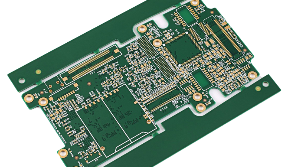
Buried vias are created by special methods during the PCB fabrication process. There are two main ways buried vias are constructed:
Blind Vias
A blind via starts on an outer layer and only penetrates part way into the PCB. The via bottom lands on an inner layer. Blind vias are typically created by laser drilling during fabrication.
Microvias
Microvias are small vias with diameters under 150um (0.006″) drilled with a laser. Microvias only span two adjacent layers allowing connections between layers not reachable with conventional drilling.
Buried vias are electroplated to form the copper barrel just like surface mount vias. However, special pastes and epoxies are used during lamination of the PCB layers to ensure a reliable connection is made.
Design Rules for Buried Vias
Buried vias have tighter design rules than standard vias that must be considered:
- Minimum size: Typically 0.2-0.3mm diameter due to high aspect ratio when drilling
- Minimum spacing: Up to 2-3 times the diameter to allow plating
- Aspect ratio: Should not exceed 10:1 (depth:diameter)
- Reliable layer span: Span only 1 or 2 layers, not more
- Laser drill entry points: Entry points must allow line of sight drilling
- Plating connections: Entry and exit points must have common copper for plating
Work closely with your PCB manufacturer to understand their specific design rules and capabilities for buried vias.
Best Practices for Buried Vias
Here are some best practices to follow when working with buried vias:
- Minimize the number of buried via layers spanned
- Avoid spanning non-adjacent layers if possible
- Place laser entry points intelligently to enable drilling
- Allow adequate space for via landing pads and routing
- Watch the aspect ratio depth versus hole size
- Closely follow manufacturer design rules
- Perform thorough design rule checking
- Prototype first designs with buried vias to confirm manufacturability
Reliability Considerations
While buried vias provide advantages, they also raise some reliability concerns to keep in mind:
- Thermal stress – CTE mismatch between copper and laminate can cause cracks over temperature cycles
- Process defects – Voids or lack of plating can cause opens more easily than surface vias
- Moisture absorption – Moisture can collect internally leading to popcorn cracks
- Separation forces – Forces from flexing can separate layers reducing reliability
Proper design, testing, and quality control is necessary to achieve robust buried via connections and avoid failures in the field. Consult with your manufacturer for recommended reliability testing procedures.
When to Avoid Buried Vias

There are a few situations where avoided buried vias are recommended:
- High current applications – Use through hole vias for best reliability
- High layer count designs – Cumulative via depth may exceed aspect ratio rules
- Low volume or budget designs – Added fabrication steps increase costs
- Large grid array packages – Difficult to drop vias into grid space
- Novice designers – Work with easier through hole vias first
Alternatives to Buried Vias
In cases where buried vias are not suitable, here are some alternatives to achieve similar benefits:
- Blind/buried vias – Partial depth vias stop at inner layers
- Skip vias – Route signals horizontally when layers change
- Staggered vias – Use multiple smaller vias for current capacity
- Back drills – Eliminate unused via portions after lamination
- Plugged vias – Fill unused vias to reduce stubs
- Surface mount passives – Avoid embedded passive components
- Build up dielectric – Use thin layers if microvia depth insufficient
Buried Vias for Advanced Applications
On the leading edge, buried vias enable advanced PCB applications:
- Buried capacitors – Parallel plate capacitors integrated vertically into PCB
- High density interconnects (HDI) – Microvias, fine lines, and through silicon vias for utmost density
- Any-layer HDI – Complex routing between any layers with microvias
- Embedded actives – Buried vias help integrate ICs like drivers or bridges within board layers
- EMI shielding – Solid copper planes surrounding areas are enabled by microvias
As PCB technology progresses, buried vias are becoming an enabling technique for integration, performance, and reliability gains.
Buried Via Types Comparison Table
| Via Type | Description | Size | Aspect Ratio | Layers Spanned |
|---|---|---|---|---|
| Blind Via | Starts on outer layer, ends on inner layer | >0.15mm | Up to 10:1 | 1 |
| Microvia | Laser drilled small via | <0.15mm | 6:1 | Adjacent layers |
| Buried Via | Starts and ends on inner layers | >0.15mm | Up to 10:1 | 1-2 |
Conclusion
While requiring tighter design rules, buried vias offer tangible benefits like reduced congestion, improved signal integrity, noise isolation, and enabling advanced integration techniques. By following best practices around manufacturability, performance, and reliability, PCB designers can take full advantage of buried vias. Close collaboration with your board fabrication partner is key to designing robust boards with buried vias.
Frequently Asked Questions
What are the key benefits of using buried vias?
The main benefits of buried vias are reduced congestion on outer layers, improved signal integrity, enablement of advanced component integration, noise isolation, and reduced stub effects versus through hole vias.
What are the main reliability risks to watch for with buried vias?
Key reliability risks with buried vias are thermal stresses leading to cracks, plating voids causing opens, moisture absorption and separation forces reducing layer adhesion over time. Proper design, testing, and quality control is necessary.
When is it best to avoid using buried vias?
Avoid buried vias in high current applications, boards with high layer counts, low volume/budget designs, large BGA packages, and when working as a novice designer. In these cases, through-hole vias or other approaches may work better.
What are the most important buried via design rules to follow?
Critical design rules are minimum size, spacing, aspect ratio limits, controlling the number of spanned layers, intelligent entry/exit placement, allowing room for landing pads, following manufacturer guidelines, and thorough DRC.
How can you create buried vias without laser drilling?
Blind/buried mechanical drilling is an alternative where vias start and stop on inner layers. Plating connections can be made through outer layer pads overlapping the blind via. This avoids the need for microvia laser drilling in some cases.
Leave a Reply