
Introduction
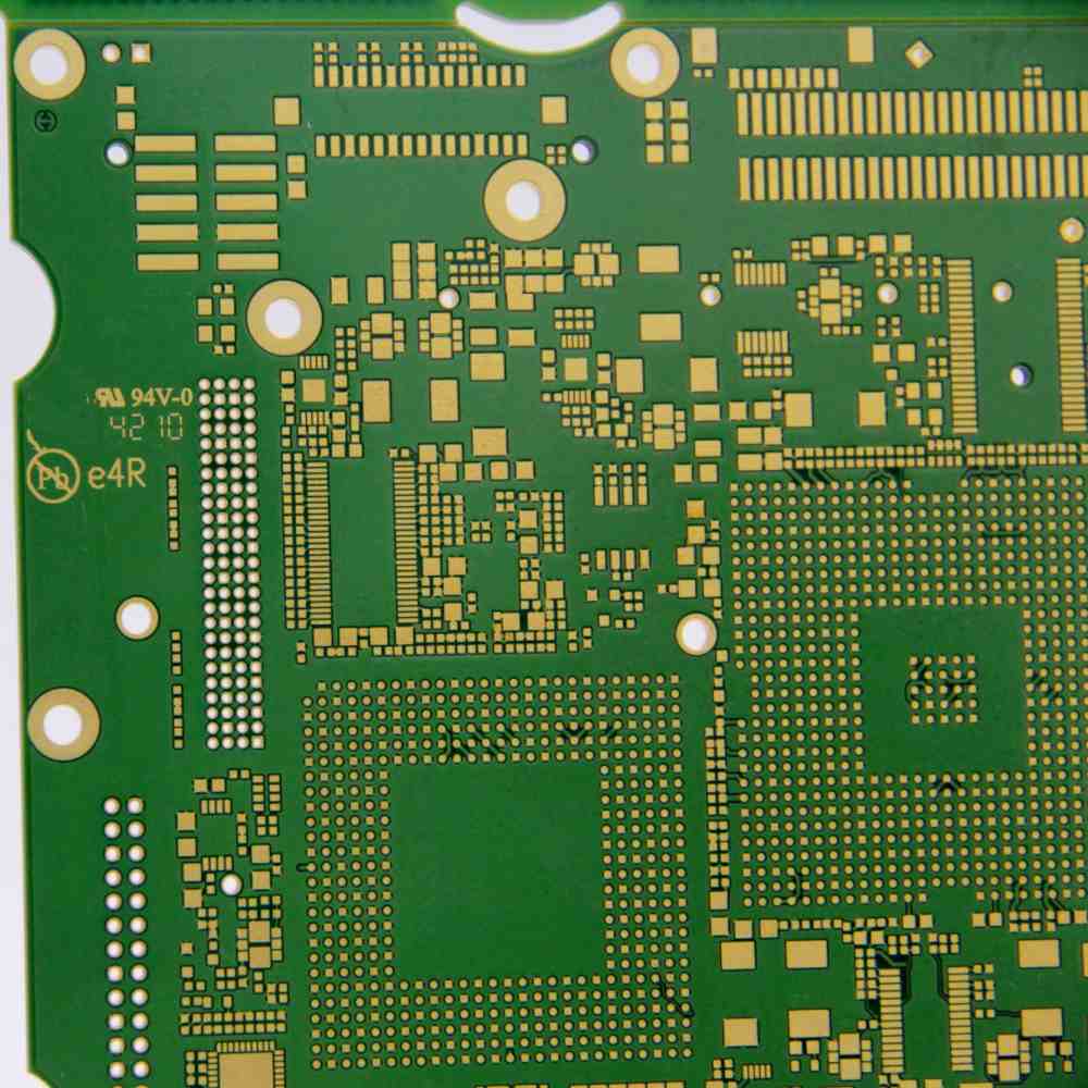
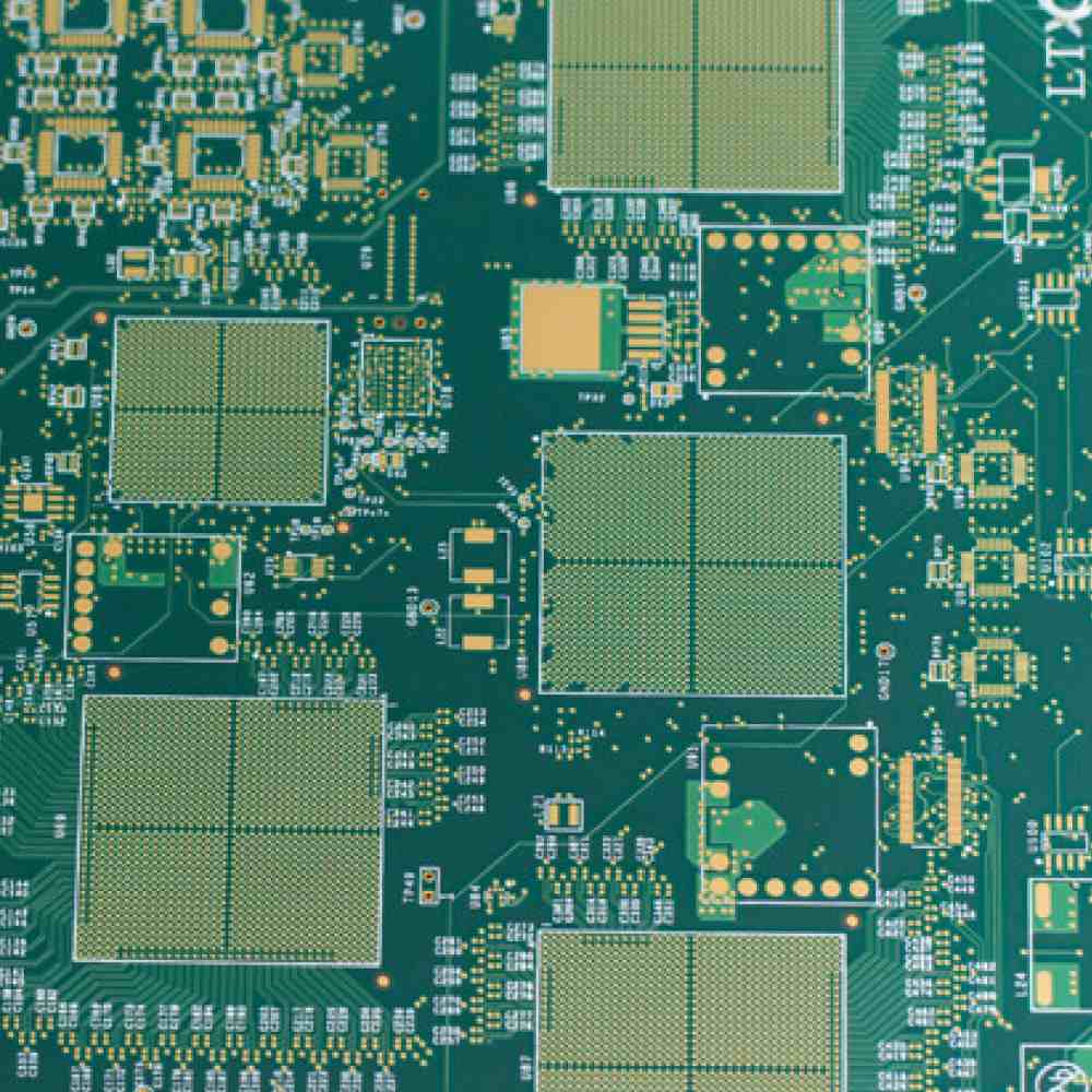
Blind vias are an essential part of many printed circuit board (PCB) designs today. As PCBs grow denser and more complex, blind vias allow connections between layers without using up valuable surface real estate. However, there are costs associated with incorporating blind vias that designers should understand thoroughly before deciding to use them. In this article, we’ll examine the pros and cons of blind vias and provide guidance on calculating the true cost of adding them to your PCB design.
What Are Blind Vias?
A blind via is a hole that connects two or more layers of a PCB without penetrating completely through the entire board. Blind vias are classified based on which layers they connect:
- Blind via – Connects an outer layer to one or more inner layers
- Buried via – Connects two or more inner layers without connecting to an outer layer
Blind and buried vias are used to route connections on a PCB while only consuming space on the layers that require interconnection. This allows PCB designers to route traces and place components on the outer layers more efficiently.
Here is an illustration of the different types of vias:
| Via Type | Description |
|---|---|
| Through Via | Connects two or more layers by penetrating fully through the PCB |
| Blind Via | Connects an outer layer to one or more inner layers |
| Buried Via | Connects two or more inner layers without connecting to an outer layer |
The Benefits of Using Blind Vias
Here are some of the advantages blind vias offer:
- Higher routing density – By only occupying space on the layers that need interconnection, blind vias allow more efficient use of surface area for trace routing and component placement.
- Lower layer count – Blind vias allow designers to connect layers internally without having to add more layers just for routing purposes. This helps reduce overall PCB thickness and cost.
- Signal isolation – Blind vias contain signals internally, preventing crossover and coupling with signals on outer layers. This helps maintain signal integrity in dense designs.
- More layout flexibility – Blind vias give designers more freedom with component placement since traces can jog internally between layers rather than having to be routed completely on one layer.
In summary, blind vias are a very useful tool for PCB designers looking to optimize board layout for density, cost, and performance. However, there are some downsides to consider as well.
The Downsides of Blind Vias
While blind vias have some clear benefits, they also come with some disadvantages and costs:
1. Increased Fabrication Cost
Blind vias require more advanced drilling and plating processes than standard through vias. This means they add cost to the board fabrication process, usually $0.02 to $0.05 more per blind/buried via compared to a through via. While not hugely substantial on a per-via basis, this can add up quickly for boards with hundreds or thousands of blind vias.
2. More Complex PCB Testing
Since blind vias cannot be probed or visually inspected from the outer layers, they require more complex testing procedures. Impedance testing, flying probe testing, and microsectioning may be necessary to ensure blind vias have been properly formed and plated through. Again, this adds time and cost to the post-fabrication process.
3. Potential Reliability Risks
The hidden nature of blind vias can potentially reduce long-term reliability if defects go undetected. Voids in the plating or weak inner layer connections won’t be identified unless extensive testing is performed. This may lead to latent defects making it through assembly and manifesting themselves later in the product lifecycle through things like thermal cycling or mechanical stress.
4. Makes Rework and Repair Difficult
If rework or repair is needed on a board with blind vias, it becomes much more challenging because the vias can’t easily be accessed from the outer layers. Fixing issues like solder bridging or replacing damaged components ends up requiring removing and replacing multiple layers of the PCB.
How to Calculate Total Blind Via Costs
To determine whether the benefits of blind vias outweigh the costs for your particular design, you need to calculate total blind via costs. Here are the key factors to include in your analysis:
1. Added Fab Cost Per Board
Calculate the total number of blind/buried vias required. Multiply this by the added cost per blind/buried via quoted by your board fabrication shop (typically $0.02 to $0.05 each). This gives you the added fabrication cost per board due to blind vias.
2. Added Testing Cost Per Board
Consult your assembly shop on what additional testing and inspection processes will be required to qualify boards with blind vias. Get quotes for any additional testing like impedance testing, flying probe testing, or microsectioning. Factor the added costs of these processes into your per-board testing cost increase.
3. Reliability Risks
Assign potential costs to increased warranty returns or rework due to latent defects from blind vias. You can start with conservative estimates of things like 1-2% additional returns and then sensitivity test those numbers during analysis.
4. Rework and Repair Costs
Estimate expenses related to more difficult board-level rework and repair when using blind vias. This may include costs for scrapping boards entirely and replacing them versus repairing them. It also includes opportunity costs related to production downtime.
5. Layer Count Savings
Factor in savings from potentially reducing layer count through use of blind vias instead of adding layers only for routing purposes. The cost per layer will depend on board thickness, fabrication process, and order quantities.
Once you have quantified all of these cost factors, you can combine them into a total cost model for blind vias that accounts for both benefits and downsides. This model allows you to dial in your specific design parameters and make an informed decision about using blind vias.
Here is an example blind via cost calculation:
| Cost Factor | Calculation | Cost |
|---|---|---|
| Blind Via Fab Cost | 2000 vias x $0.05 per via | $100 |
| Added Testing | $250 per board | $250 |
| Yield Loss (1%) | 100 boards x 1%=$1 per board | $100 |
| Rework Costs | $50 per board for 5% rework rate | $25 |
| Layer Count Savings | -4 layers x $1000 per layer | -$4000 |
| Total Added Cost Per Board | -$3525 |
In this example, the use of blind vias to eliminate 4 layers reduces total board costs by $3525 per board. This indicates the project benefits financially from using blind vias.
Always be sure to sensitivity test your key assumptions like failure rates to account for uncertainty in the model. But following this approach allows you to numerically evaluate the blind via tradeoffs.
Design Tips to Minimize Blind Via Costs
If your analysis shows blind vias are cost-effective for your particular design, here are some tips to minimize their downsides:
- Minimize total number of blind vias used. Be selective about only using them where layout would otherwise be highly sub-optimal.
- Increase blind via capture pad sizes slightly to provide more margin in drilling accuracy.
- Perform stackup analysis to ensure reliable plating through all blind via barrels.
- Where possible, make blind vias accessible for probing by having them connect to test points or vias that penetrate the outer layers.
- Group blind vias together into “via farms” to simplify rework if needed.
- Follow all manufacturer DRC rules and employ adequate via-in-pad rules.
- Perform thorough post-fabrication electrical testing like flying probe testing and microsectioning to catch any latent defects.
Conclusion
Adding blind vias provides many benefits but also incurs costs related to fabrication, testing, risk, and rework. By carefully calculating total cost impacts using the guidelines provided, PCB designers can determine when blind vias make sense and implement them in a reliable, cost-effective manner. Leveraging blind vias strategically allows you to fully exploit the layer-to-layer routing possibilities of complex, multilayer boards and optimize your layouts.
FAQ
Why are blind vias more expensive to fabricate than through vias?
Blind vias require more complex drilling and plating processes. Drill bits have to stop partway through the PCB and additional steps are needed to electroplate the inner barrel surfaces. By contrast, through vias can be drilled straight through and plated in simpler barrel plating tanks.
How much does impedance testing for blind vias typically cost?
The cost for impedance testing for blind vias can range from $50 to $500 per board depending on test coverage. Testing is typically performed using automated test systems like those from Agilent, Acculogic or Seica. Costs increase with the number of test points.
What are some ways to reduce blind via fabrication costs?
Using laser-drilled microvias can eliminate the cost premium compared to through vias. Also, work with your fabricator to optimize the plate-through process – more reliable plating lowers rework rates which saves money. Finally, minimizing the total number of blind vias used on the board will help.
When does it make sense to add a layer instead of using blind vias?
Adding a layer may be more cost-effective if the layer count is already low, density is very high, and the additional layer significantly reduces via counts. In high quantity orders, the cost per added layer is usually lower compared to adding many expensive blind vias.
What design changes can reduce the risks of defects with blind vias?
Increasing capture pad sizes, following all manufacturer DRC guidelines, using redundant vias, and adding test points connected to blind vias can help minimize the risks. It’s critical to work closely with your fabrication shop to design reliability into the process.


Leave a Reply