What are Blind Vias?
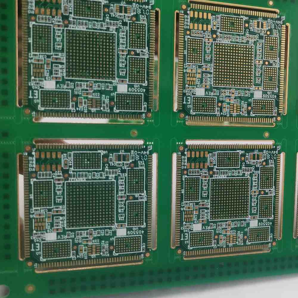
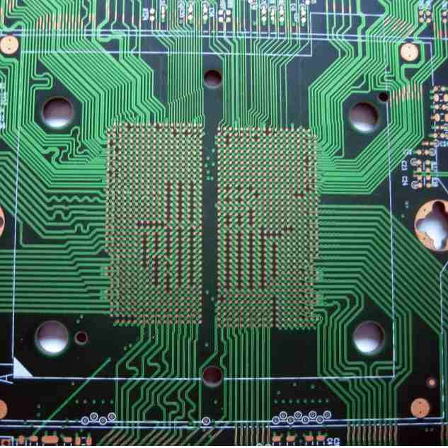
Blind vias, also known as buried vias, are plated through-holes in a printed circuit board (PCB) that connect internal layers without being visible or accessible from the outer layers. Unlike standard through-hole vias which span the entire board, blind vias start and stop within the internal layers of the board.
Blind vias play an important role in allowing signals to travel between internal layers for high density interconnects (HDI) boards. They help minimize layer-to-layer distances and enable optimal trace routing.
Key Characteristics of Blind Vias
- Connect two or more internal layers without connecting to the outer layers
- Not visible from the surface of the PCB
- Often used in conjunction with microvias
- Requires specialized drilling and plating processes
- Allow high-density routing between layers
- Help minimize stub lengths
Why Use Blind Vias?
There are several key benefits that make blind vias a useful tool for PCB designers:
Increased Routing Density
Blind vias allow connections between internal layers without taking up space on the outer layers. This enables higher routing density and complex connectivity between layers.
Shorter Trace Lengths
By skipping the outer layers, blind vias provide shorter paths for signals to travel between internal layers. This minimizes undesirable effects like reflection, attenuation, and crosstalk.
Better High-Speed Performance
The shorter trace lengths enabled by blind vias are especially beneficial for high-speed signals. They allow signals to propagate faster and with less distortion.
Improved Impedance Control
Blind vias allow traces to reference a continuous ground or power plane over their entire length. This helps maintain proper impedance control for high-speed signals.
Reduced EMI/RFI
Keeping high-speed traces buried inside the board reduces unwanted electromagnetic interference (EMI) and radio frequency interference (RFI).
| Benefits of Using Blind Vias | |
|---|---|
| Increased routing density | Allows more interconnects between layers |
| Shorter trace lengths | Minimizes signal degradation |
| Improved signal integrity | Essential for high-speed designs |
| Consistent impedance | Aids impedance matching |
| Reduced EMI/RFI | Lessens interference |
Design Considerations for Blind Vias

Although blind vias provide many benefits, they also introduce some design considerations:
Layer Planning
With blind vias, you lose the ability to freely route signals between any two layers. Layer planning is critical to defining viable blind via connections.
Via Capturing
Vias between inner layers may require capture pads on adjacent layers for soldering if any connections are needed post-assembly.
Stackup Dependencies
Your board stackup will determine the layer combinations available for blind vias based on core thicknesses.
Fabrication Complexity
Blind vias require specialized drilling and plating equipment, adding cost and cycle time compared to standard vias.
Testing Limitations
It’s not possible to physically probe blind vias from the outer surfaces, complicating testing and debugging.
| Design Considerations for Blind Vias | |
|---|---|
| Layer planning | Determine viable layer connections |
| Capture pads | May be needed for soldering |
| Stackup dependencies | Limit layer combinations |
| Fabrication complexity | Increases costs and cycle time |
| Testing limitations | Probing not possible from surface |
How Are Blind Vias Fabricated?
Fabricating blind vias requires advanced PCB manufacturing capabilities:
Laser Drilling
A laser is used to selectively ablate material to drill vias between specific layers without penetrating the entire board.
Plating
Electroless copper plating coats the interior of the blind via holes, followed by electroplating to build up the appropriate copper thickness.
Filling
The blind vias are filled flush with the inner layer pad surface, typically using epoxy or a plugging process.
Outer Layers
Outer layer circuitry is processed on the board without affecting the buried blind vias.
| Blind Via Fabrication Process | |
|---|---|
| Laser drilling | Selectively ablates inner layer material |
| Plating | Electroless then electroplating |
| Filling | Epoxy or plugging process |
| Outer layer processing | Performed after blind vias complete |
The specialized equipment and additional processing steps increase the complexity and cost of boards with blind vias, but enable the performance benefits they provide.
Design Rules for Blind Vias
Here are some key design rules to follow when working with blind vias:
- Minimum size – Typically 0.15-0.20mm due to laser drilling limitations
- Maximum aspect ratio – Limit the ratio of hole depth to diameter (e.g. 5:1)
- Minimum annular ring – Allow sufficient margin on pad sizes for inner layer alignment
- Layer transitions – Avoid abrupt transitions between layers connected with blind vias
- Anti-pad size – Provide sufficient clearance around blind vias for filling
- Fill requirements – Specify fill type (epoxy, copper plug) based on conductivity needs
Careful adherence to manufacturer design rules ensures your blind vias can be properly fabricated. Rules may vary between different PCB shops.
Blind Via Applications
Some common applications that benefit from the use of blind vias:
- High density interconnect (HDI) – Blind vias allow extremely dense routing between layers in portable and mobile devices.
- High speed design – Shorter connections improve signal integrity for fast digital circuits and RF applications.
- Mixed signal – Buried vias isolate sensitive analog signals from noisy digital signals.
- EMI control – Containing signals inside the board reduces undesirable emissions.
- Complex power distribution – Power and ground networks can be distributed between layers using blind vias.
- Dense component mounting – Allows connections below tightly spaced components.
Comparison to Other Via Types
Microvias
Like blind vias, microvias provide connections between internal layers without penetrating the full board thickness. The key difference is that microvias have a much smaller diameter, typically under 0.15mm.
Buried Vias
Buried vias connect internal layers and are also covered by outer layer laminations. But unlike blind vias, they cannot be filled and plated since they are completely covered.
Standard Through-Hole Vias
Standard vias span the full thickness of the board to interconnect all layers. Though simpler to manufacture, they have poorer signal integrity compared to blind vias.
| Via Type Comparison | ||
|---|---|---|
| Via Type | Diameter Range | Layers Connected |
| Blind | 0.15mm and above | Between internal layers |
| Micro | Under 0.15mm | Between internal layers |
| Buried | Any size | Between internal layers |
| Standard | Any size | All layers |
When to Use Blind Vias
Here are some guidelines on when to use blind vias:
✓ For high density interconnections between internal layers
✓ When signals need to reference inner plane layers
✓ To reduce stub lengths for high speed signals
✓ If minimizing EMI emissions is critical
✓ For RF and controlled impedance signals
✓ To isolate sensitive analog signals
✽ Avoid blind vias if design simplicity is priority
✽ Not suitable if probing internal nets is needed
✽ Adds cost when standard vias would suffice
In summary, blind vias are a useful tool for high performance and high density PCBs, providing shorter connections between internal layers when designed properly. Evaluate their benefits against the increased fabrication complexity.
Frequently Asked Questions (FQA) About Blind Vias
What are some typical blind via sizes?
Blind via sizes typically range from 0.15mm to 0.25mm in diameter due to the limitations of laser drilling technology used to create them. The maximum aspect ratio (depth to diameter) is usually around 5:1.
How are blind vias aligned between layers?
The blind via holes are laser drilled using an extremely accurate laser system capable of calibrating to fiducials and targets on each inner layer. This allows precision alignment between layers.
Can microvias be combined with blind vias?
Yes, microvias with diameters under 0.15mm are often used to connect blind vias between additional inner layers when even denser interconnections are needed.
Are there limitations on blind via placement?
Avoid placing blind vias underneath ball grid array (BGA) packages or other components that cannot accommodate an inner layer pad. Also keep blind vias away from board edges that could impact drilling.
How do blind vias impact board cost?
The specialized laser drilling and plating required for blind vias increases fabrication cost and cycle time compared to standard plated through holes. But they enable significant improvements in circuit density, performance and reliability.


Leave a Reply