Introduction
Printed circuit boards (PCBs) are essential components in virtually all modern electronics. They provide the physical structure and electrical connections between components in an electronic device. A key part of PCB design and manufacturing is creating vias – holes that connect different layers of copper traces in the board. Blind vias are a specific type of via that connect an internal layer of a PCB to an external layer, without going through the entire board. Blind vias enable more complex routing while taking up less space than through-hole vias. This article will provide an in-depth look at the blind via manufacturing process for PCBs.
What are Blind Vias?
Blind vias are holes made in a PCB that only go partway through the board, connecting an internal layer to a surface layer. They differ from through-hole vias that go through the entire board from top to bottom. The key benefits of using blind vias include:
- More routing flexibility – Allows connecting inner layers without using up surface space
- Higher component density – Takes up less space compared to through-hole vias
- Improved signal integrity – Shorter path means less signal degradation between layers
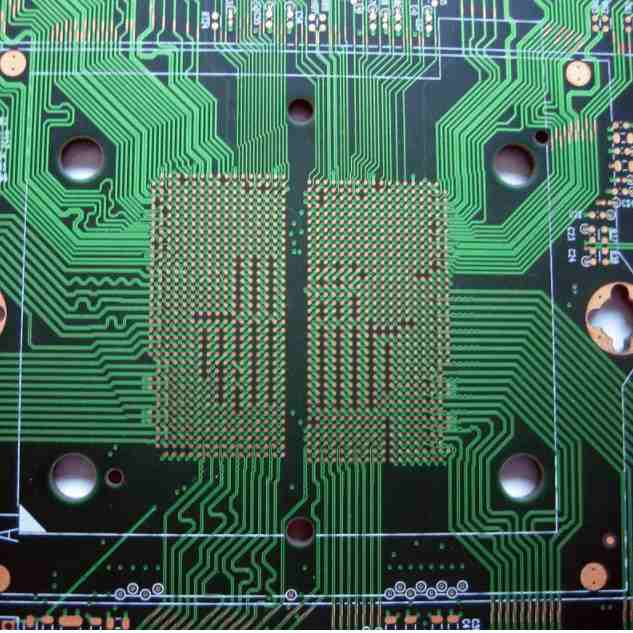
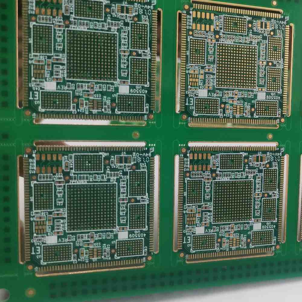
Blind vias are essential for complex, multilayer PCB designs. High density interconnects (HDI) technology relies heavily on blind/buried vias to connect component pads and routing layers.
Blind Via Manufacturing Process Steps

Creating reliable blind vias requires precision machining and plating. Here are the key steps:
Drilling
The first step is to mechanically drill holes at the specified locations on the PCB stackup. For blind vias, high precision drilling is required to control the hole depth. Laser drilling is also sometimes used to create blind vias, which allows even more accuracy. The drilling process results in an open hole connecting the two conductive layers.
Desmear
After drilling, the blind via holes typically go through a desmear process. This involves using chemicals to remove resin smear from the hole walls created during drilling. Removing the resin smear helps ensure good conductivity and adhesion during plating.
Plating
A conductive plating is then applied to the blind via holes to form the electrical connection between layers. Electrolytic copper plating is most commonly used to plate the blind vias. A thin seed layer of copper is first deposited over the entire PCB surface. Then current is applied to electroplate copper just within the via holes.
Outer Copper Layer Subtractive Etching
Once plated, the outer copper layers go through a subtractive etching process to remove copper and define the traces and pads. The plated blind vias are protected from etching using a dry film or liquid photo resist. This leaves the plated vias electrically connected between layers.
Backfilling
In some cases, blind vias are backfilled after plating. This involves filling them with epoxy or other dielectric material. Backfilling provides extra structural support and helps prevent solder wicking down into the vias.
Key Factors for Reliable Blind Vias
Producing robust, reliable blind vias requires optimizing several key factors:
- Via wall smoothness – Adequate desmear is critical to ensure good plating adhesion. Rough via walls can lead to poor connections.
- Accurate depth control – Drilling precision is essential to control how deep vias connect between layers.
- Plating thickness – Must have adequate copper thickness for low resistance, high current capacity connections.
- Backfill void avoidance – Preventing gaps or voids in via backfilling material prevents reliability issues under thermal cycling.
- Registration – Drilled holes must align precisely with pad and trace locations on each layer.
Careful process control and validation testing helps ensure these factors are optimized to produce reliable blind vias.
Applications of Blind Vias
Blind vias enable many important PCB applications:
High Density Interconnects
HDI technologies rely heavily on blind/buried vias to route connections between dense component pads. This allows fitment of complex wiring in a small form factor.
RF Circuits
In RF designs, blind vias can provide direct connections between components and ground/power planes. This optimizes signal integrity at high frequencies.
Multi-Layer Boards
Blind vias are essential in boards with 4+ layers to enable interconnections between inner layer traces.
IC Package Interposers
Multi-layer interposers that interface ICs to a PCB often leverage blind/buried vias for high density vertical connections.
LED Circuit Boards
LED PCBs often use blind/buried vias to connect top side LED pads to inner layer ground planes.
Conclusion
Blind vias enable complex, high density PCB designs by allowing vertical connections between inner board layers. Creating reliable blind via connections relies on precision drilling and plating processes. When optimized, blind vias provide performance benefits in RF, HDI, and multilayer circuits. They will continue to play a key role in advancing PCB technology for electronic devices and systems.
Frequently Asked Questions
What is the key difference between a blind via and a buried via?
The main difference is that a blind via connects an inner layer to an outer layer, while a buried via connects two or more inner layers without connecting to a surface layer. Buried vias are completely internal to the PCB.
What drilling methods can be used to create blind vias?
Mechanical drilling and laser drilling are the two main methods used for blind via holes in PCB fabrication. Mechanical drilling offers lower cost but laser drilling provides more precision.
Why is desmear important for blind vias?
Desmear removes the resin smear deposited on via hole walls during drilling. This resin can impede plating adhesion and conductivity if not removed, causing potential reliability issues.
How are blind vias aligned to pads and traces?
A pattern recognition system is used to optically align the drilled holes to the pad and trace locations on each layer based on artwork data. Tight registration tolerances are necessary.
Can stacked and staggered vias be implemented using blind/buried vias?
Yes, stacked and staggered via configurations are often implemented with blind/buried vias to optimize routing density and minimize layer transitions.


Leave a Reply