What are Blind Vias in PCBs?
A blind via is a plated hole that connects different layers of a printed circuit board (PCB) without going all the way through the entire board. Blind vias connect an inner layer to an outer layer, stopping before they reach the opposite outer layer. They are called “blind” because one of the outer layers is not able to “see” the hole.
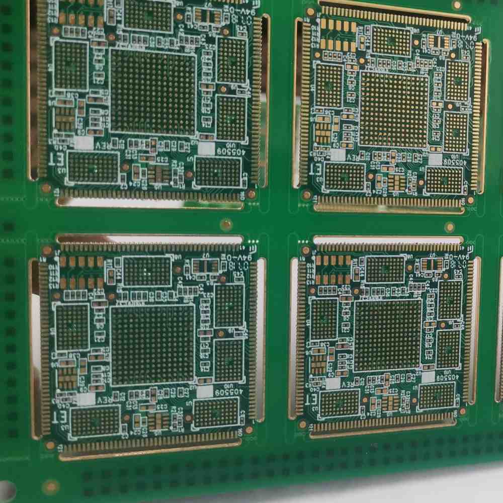
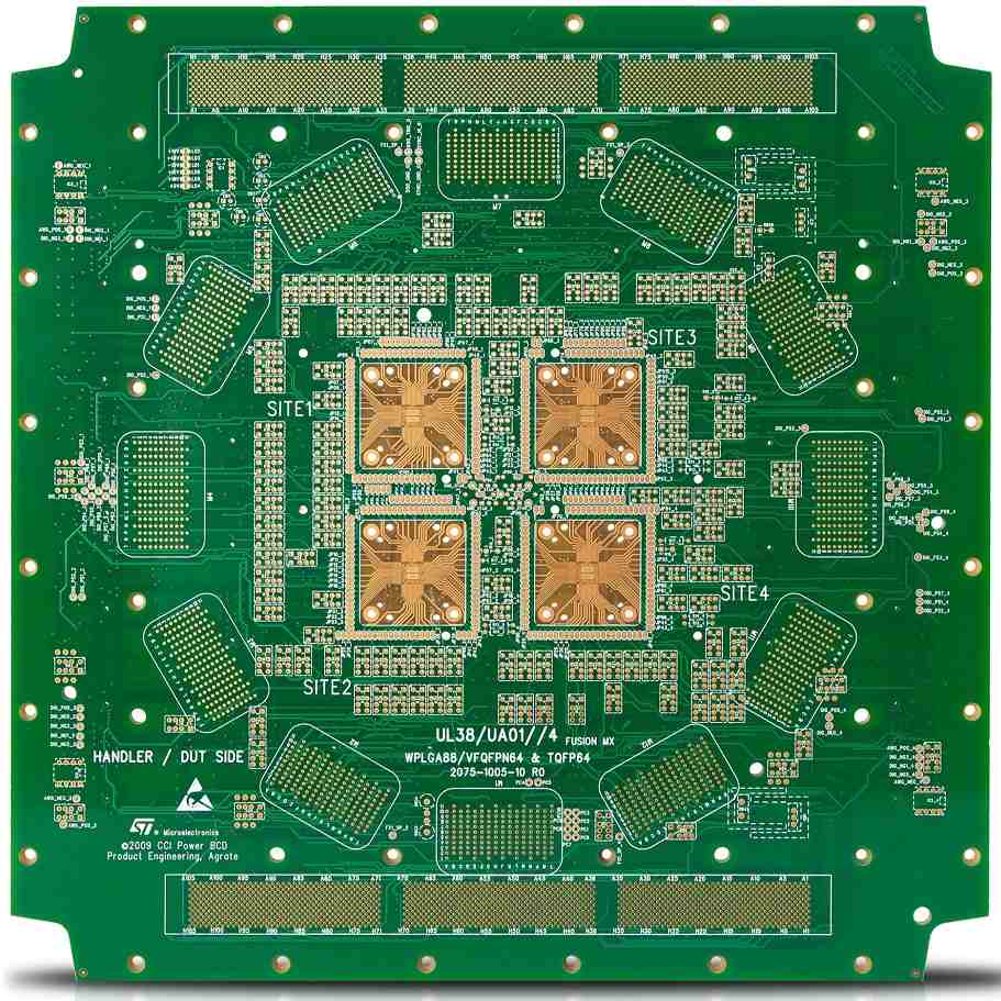
Blind vias are an important part of high-density interconnect (HDI) PCB designs as they allow routing between layers that would otherwise be inaccessible with only through-hole vias. By using blind vias, designers can make fuller use of the board layers, reduce layer transitions, and achieve higher component densities.
Key Characteristics of Blind Vias
- Connect an inner layer to an outer layer
- Do not go through the entire PCB stackup
- Allow higher routing density
- Enable layer transitions without using through vias
- Require specialized drilling and plating processes
Why Use Blind Vias? Benefits and Applications
There are several key benefits that make blind vias a useful tool for advanced PCB designs:
Higher Routing Density
Because blind vias do not go through all layers, they take up less space and allow tighter routing than through-hole vias. This enables higher component densities.
Reduced Layer Transitions
Blind vias minimize the need to transition through multiple layers to access different routing planes. This simplifies routing.
Improved Signal Integrity
With shorter drill lengths than through vias, blind vias have less capacitance and inductance, giving better signal performance at high speeds or frequencies.
Buried Component Access
Blind vias provide access to components placed between layers without using up space on the outer layers.
Reasons to Use Blind Vias:
- HDI PCBs with high component densities
- Boards requiring tight space constraints
- High-speed digital and RF designs
- Complex multilayer boards with buried components
- Minimizing layer transitions for ease of routing
How are Blind Vias Constructed?
Constructing blind vias requires specialized drilling and plating processes compared to through-hole vias. Here are the main steps:
1. Drilling
The PCB manufacturer drills holes partially through the PCB using advanced drilling equipment. Common techniques include laser drilling or mechanical drilling with depth control.
2. Plating
Thewalls of the blind via holes are plated with copper, usually using electroless plating followed by electroplating. This creates a conductive path between the connected layers.
3. Layer Alignment
The layers are precisely aligned so the blind vias correctly connect the intended padsin each layer. Photolithography transfers the pad outlines onto each layer.
4. Outer Pad Plating
The outer pads are plated with solder or metals to allow component terminations. There are no pads on layers the vias do not pass through.
5. Solder Mask
A solder mask coats the finished board, leaving the pads exposed. The blind vias are now completed.
Blind Via Design Rules and Limitations
There are some important guidelines and limitations to consider when designing blind vias:
- Minimum blind via diameter – Typically 0.1-0.15mm due to reliable plating limits.
- Maximum aspect ratio – Blind via depth shouldn’t exceed 5-8x their diameter to avoid reliability issues.
- Nearest neighbor spacing – Adequate spacing between vias avoids plating issues.
- Pad size – Outer pads are often enlarged to allow for layer misalignment tolerance.
- Layer Pairs – Blind vias only connect two adjacent layers due to fabrication limitations.
- Signal Layers – It’s best to only use them between signal layers, avoiding blind vias between plane layers.
Additional Considerations:
- Thermal design – Blind vias don’t conduct heat as well as through vias.
- Fabrication cost – More complex process compared to through vias.
- Testing – Require special test access points.
- Reliability – Potential problems from poor plating and high aspect ratios.
Following design guidelines and manufacturer capabilities is key to using blind vias effectively.
Example Applications of Blind Vias
Here are a few practical examples of using blind vias in PCB designs:
1. Dense BGA Routing
Blind vias allow escaping dense ball grid array (BGA) pads to internal layers without consuming space on the outer layers. This maximizes routing real estate.
2. RF Transitions
In high frequency RF designs, blind vias make transitions between closely spaced signal layers without disrupting ground planes. This maintains signal integrity.
3. Buried Passive Components
Capacitors or resistors can be placed between internal layers and connected with blind vias. This saves space compared to surface mount passives.
4. IC Power Delivery
Power and ground nets can be distributed on internal planes using blind vias without multiple through-hole transitions.
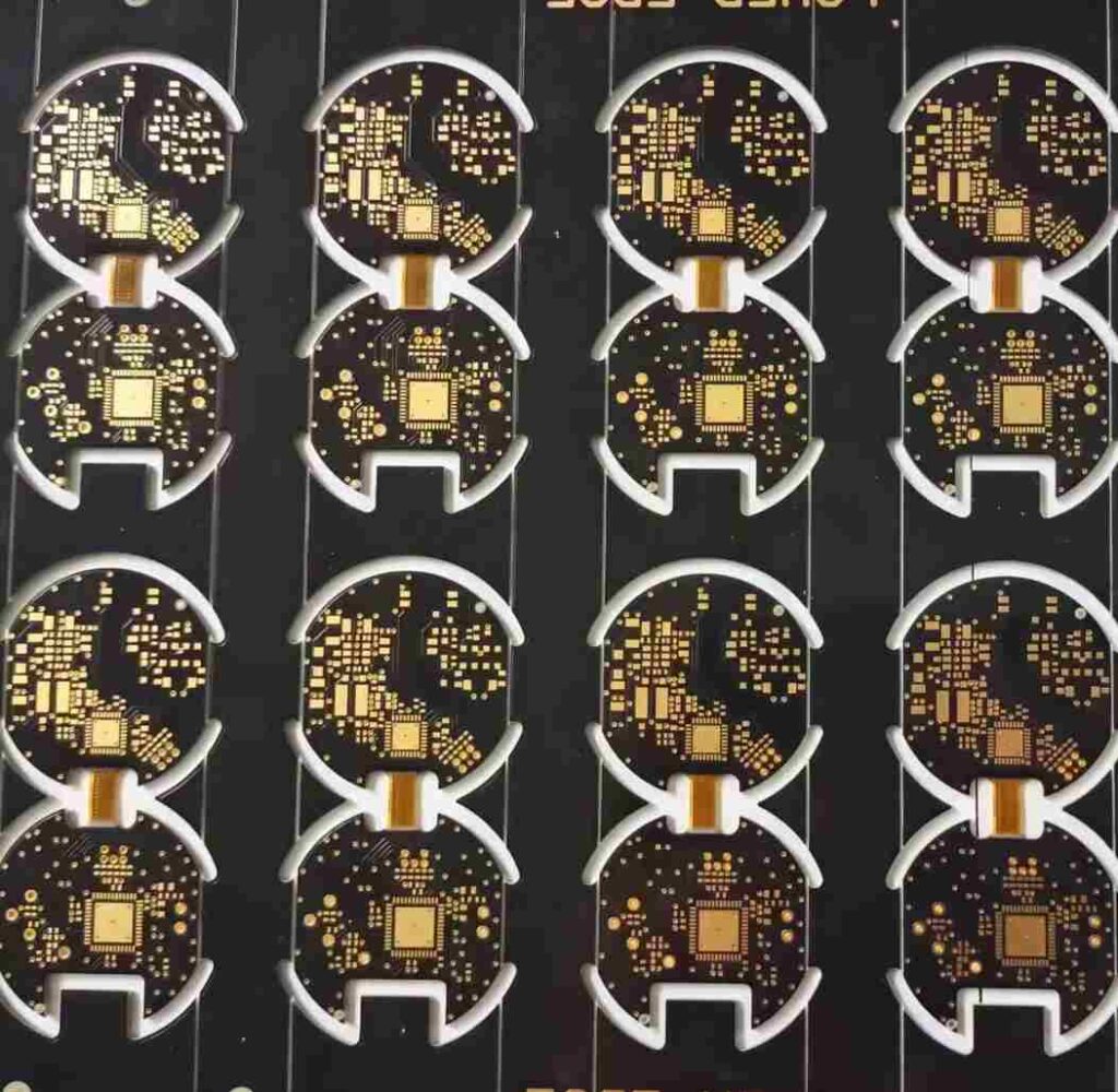
5. Board Interposers
High-density board-to-board connectors employ blind vias to route signals between the top and bottom of interposer boards.
Blind and Buried Vias – What’s the Difference?
There is an important distinction between blind vias and buried vias:
- Blind vias connect an inner layer to an outer layer. The hole is blind from one side.
- Buried vias connect two or more inner layers without connecting to either outer layer. The hole is unseen from outside the PCB.
Buried vias take the concepts of blind vias a step further for even denser HDI designs. But they require very complex lamination and drilling processes.
Summary of Key Points on Blind Vias
To summarize, the key points on blind vias in PCBs are:
- Connect inner to outer layers without passing through the entire board.
- Enable higher routing density versus through vias.
- Allow access to internal layers without consuming outer layer space.
- Require specialized drilling and plating fabrication processes.
- Follow design rules for reliable performance.
- Widely used in multilayer and HDI boards to utilize all layers efficiently.
- Provide benefits like reduced noise and tighter layouts.
Blind vias open up possibilities beyond just using through vias, supporting sophisticated PCB designs and high-performance applications.
Common Usage Scenarios for Blind Vias:
- High density BGA fanout routing
- Making layer transitions in RF circuits
- Accessing buried components like capacitors
- Routing power distribution networks internally
- Interconnecting stacked vias in HDI boards
FAQ on Blind Vias
Here are answers to some frequently asked questions about blind vias:
Q: Can you stack blind vias?
A: Yes, blind vias can be stacked to route between non-adjacent layers. A series of stacked blind vias connects inner layers to each other. The total length is still shorter than a through via.
Q: Are there size limits on blind vias?
A: The fabrication process imposes a minimum size around 0.1mm. There are also aspect ratio limits since too deep a blind via risks reliability problems. Typical max ratios are 5:1 to 8:1.
Q: Do blind vias improve signal integrity?
A: Generally yes. The shorter path than a through via gives blind vias less parasitic inductance and capacitance. This provides better performance for high-speed or high-frequency signals.
Q: Can I place components in blind vias?
A: It’s challenging but possible. Components like chip capacitors or resistors can be embedded between layers if the design provides space in the blind via. This requires a cavity in the hole.
Q: Are blind vias more expensive to fabricate?
A: Yes, the specialized drilling and plating processes required for blind vias increase fabrication costs compared to through vias. But the benefits often justify the extra expense.


Leave a Reply