Introduction to Blind Vias in Pads
A blind via is a hole that connects different layers of a multilayer printed circuit board (PCB) without going all the way through the entire board. Blind vias are often used in pad designs, allowing connections between the pad and internal layers while avoiding drilling completely through the board. This offers several advantages:
- Reduced drilling costs – Only drilling to necessary depths instead of all the way through the board
- Allows higher pad densities – Avoiding surfacemount pad violations from through-hole vias
- Improved signal integrity – Removing stubs that could cause reflections in high-speed signals
- Layer stackup flexibility – Change internal layers without affecting external pads and vias
In particular, incorporating blind vias into surface mount pads connects the component pins to inner layer traces while keeping the pad clear of plated through holes. This article provides a detailed overview of blind vias in pads, examining the applications, pros and cons, design considerations, and manufacturing processes.
Applications of Blind Vias in Pads
Blind vias in pads are commonly used in these types of PCBs:
- High density interconnect (HDI) – With microvias connecting finely spaced pads to internal layers
- RF/microwave boards – Avoiding stubs by using buried vias underneath components
- LED lighting – Optimized layer usage with blind/buried vias under LEDs
- Mixed technology – Combining blind vias with through-hole components
- Multi-layer boards – Allowing flexible internal layer circuitry under surface mount footprints
Here are some specific examples of using blind vias in pads:
- BGA package – A ball grid array package with a blind via under each ball connecting to internal power and ground planes.
- QFN package – A quad flat no-lead package with a blind via in each thermal pad.
- RFIC chip – A radio frequency integrated circuit with tunable blind vias under each input/output.
- LED array – High density blind vias connecting LED pins to internal driver circuitry.
- Mixed SMT/PTH – A board with blind vias under SMT components and plated through holes for connectors.
In these types of designs, blind vias allow optimized electrical performance and dense component layouts.
Pros and Cons of Blind Vias in Pads
There are several key advantages of using blind vias in pads:
Advantages
- Higher routing density under surface mount pads
- Avoid pad violations from through hole vias
- Reduced drilling costs by only drilling necessary depths
- Elimination of stubs that can cause signal reflections
- Flexibility in layer stackup and partitioning
- Solution for assembling SMT and PTH components together
However, there are also some disadvantages and considerations:
Disadvantages
- More complex design rules and DRC checking
- Requires advanced manufacturing capability
- Potential for reduced mechanical strength with microvias
- Difficult to probe or repair if unable to access blind layers
- Can complicate component replacement if pads change
- Adds complexity to soldering if via holes act as solder sumps
The advantages often outweigh the disadvantages for many advanced PCB designs. But designers should carefully evaluate their specific needs.
Key Design Considerations

Here are some key factors PCB designers should consider when planning to use blind vias in pads:
Board Density Requirements
- Are blind vias necessary to route high density pads to internal layers? Or can all connections be made with surface traces?
Manufacturing Capabilities
- Can your shop reliably produce boards with blind vias at your required budgets and volumes?
Drilling Feasibility
- Is there space in the pad design for the necessary blind via holes?
Stackup Planning
- Will you need to access internal layers that are covered by SMT pads? Plan pad/via locations carefully.
Thermal Management
- Blind vias can act as thermal conduits to inner planes. Consider for heat sinking.
Signal Integrity
- Model effects of blind vias on impedance and high speed signals. Watch for discontinuities.
Testing and Rework
- Consider probe points and repairability with blind vias. May require filling vias.
Soldering Techniques
- Will blind via holes suck solder away from pads? May need solder masks or fill.
By evaluating all these aspects up front, PCB designers can leverage the benefits of blind vias successfully.
Manufacturing Processes
Specialized fabrication processes are required to produce printed circuit boards with blind vias in pads. Here is an overview of how they are manufactured:
Drilling
- CNC laser drills or mechanical drills bore holes to the required depths. Microvias ≤ 0.15mm are typically laser drilled. Larger holes can use mechanical drills. Depth accuracy is critical.
Metallization
- Blind vias are plated with copper using electroless and electrolytic plating processes. Often requires a thin seed layer deposition by sputtering or electroless plating prior to electroplating the hole walls.
Testing
- Blind via continuity is tested electrically by probing or using automated optical inspection (AOI). Ensures plating reached required depths.
Board Fabrication
- Completed using standard PCB lamination, imaging, etch, and finish processes. Blind via PCBs typically use high TG resin and may require staggered lamination pressures.
Solder masking
- LPI solder masks are applied over pads with openings for soldering. Laser ablation can cut small openings over microvias.
With these fabrication techniques, PCB manufacturers can produce boards with blind vias terminating at precise layer depths.
Example Blind Via Pad Designs
Here are two examples of blind via pad layouts in different scenarios:
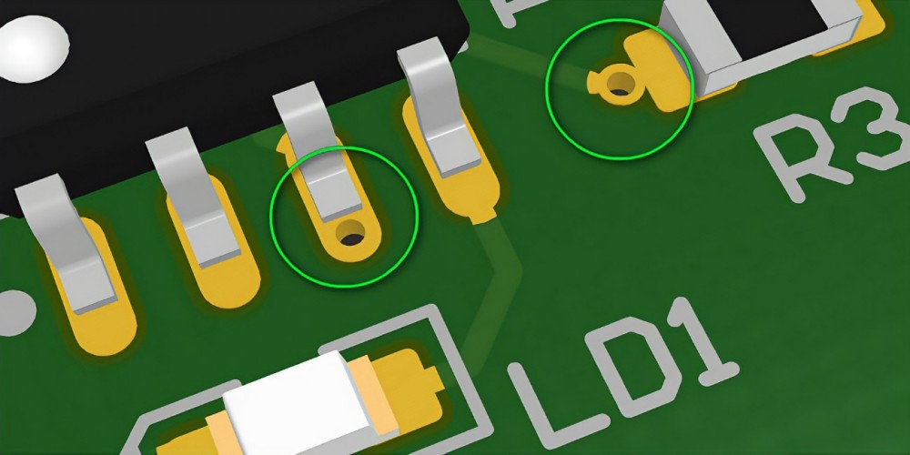
Blind Via Under QFN Package
This design uses a blind via under the center thermal pad of a QFN package:<img src=”qfn_blind_via.png” alt=”QFN Package with Blind Via in Pad” width=”300″>
- The via connects the thermal pad to an internal ground plane for heat sinking.
- This avoids a through hole via violating the pad space.
- The via has a larger diameter than the stencil opening to avoid solder wicking into the hole.
- The ground plane is on layer 2, so drilling terminates after penetrating the first dielectric layer.
Array of Blind Microvias Under BGA
Here is an example BGA footprint with an array of blind microvias under each solder ball:<img src=”bga_blind_vias.png” alt=”BGA Package with Array of Blind Microvias” width=”300″>
- The blind vias connect each ball pad to buried traces on layers 2 and 3.
- Via sizes range from 0.1mm to 0.15mm for high density wiring.
- The vias are staggered to avoid excessive pad necking from each via intrusion.
- The bury depth is controlled precisely to avoid contacting other layers.
This design achieved over 200 I/Os in a compact 10mm BGA footprint.
Blind Vias in Pads FAQ
Here are some frequently asked questions about using blind vias in pad designs:
Q: How small can you make blind via holes?
A: Laser drilling can produce blind microvias down to 0.05mm in diameter, but 0.1mm is more typical. Mechanical drilling achieves 0.15-0.2mm.
Q: Can you plug blind vias?
A: Yes, blind vias can be plugged similarly to through-hole vias using epoxy, soldermask plugs, or liquid solder. This may be done for solder control.
Q: Do boards with blind vias cost more?
A: Yes, the specialized drilling and plating does increase fabrication costs compared to standard multilayer PCBs. But this enables improved performance.
Q: Are there design rules for the ratio between hole size and pad size?
A: Generally the hole diameter should be less than 50% of the pad diameter to maintain adequate annular ring width. This varies by manufacturer.
Q: Can blind vias be repaired?
A: It is more difficult. Filled blind vias can be drilled out and re-plated. Unfilled vias require accessing the blind layer or drilling from the opposite side.
Conclusion
Blind vias under surface mount device pads provide an invaluable tool for routing density and performance in complex printed circuit board designs. By allowing connections between pads and internal layers without through-hole vias, they enable optimized layer usage, compact component layouts, reduced stub effects, and flexible fabrication. With careful planning and execution, PCB designers can take full advantage of the capabilities of blind via in pad technology.


Leave a Reply