Introduction
Printed circuit boards (PCBs) are essential components in all types of electronic devices and equipment. They provide the mechanical support and electrical connectivity for the components that make up the electronic circuitry. An important aspect of PCB design is the use of vias – plated-through holes that connect different layers of the board to allow signals and power to be routed between layers. Blind vias are a specialized type of via used in multilayer PCBs that connect an internal layer to only one external layer, rather than connecting two external layers. Blind vias provide a number of benefits in high density PCBs but also come with some unique design considerations.
What are Blind Vias?
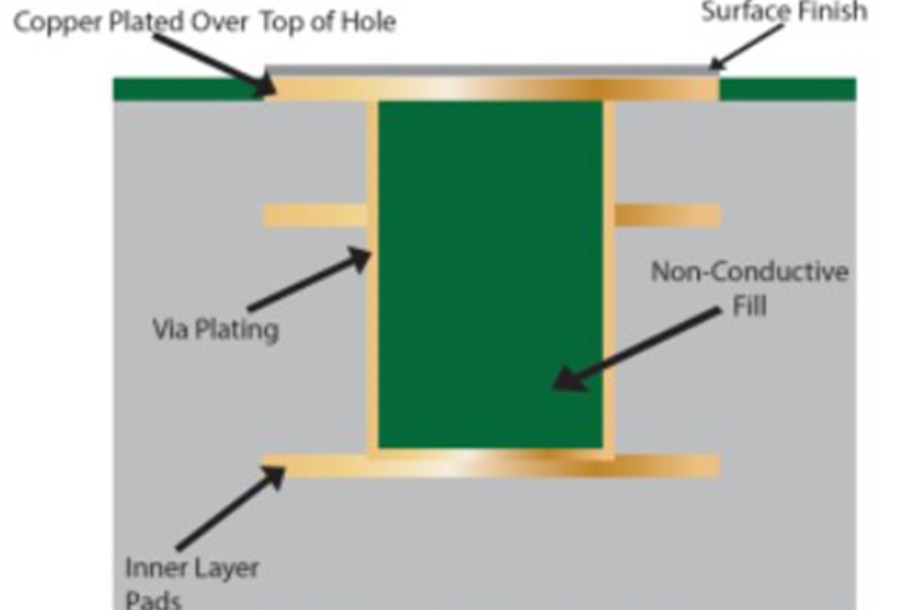
A standard through-hole via connects two or more outer layers of a PCB. In contrast, a blind via connects an internal layer to only one outer layer. For example, in a 6-layer board, a blind via may connect layer 3 to layer 1 but does not extend all the way through the board to layer 6. The key characteristics of blind vias are:
- Connect an internal layer to one outer layer.
- Do not extend fully through the PCB.
- Often filled and plated over.
- Allow routing between layers not sequentially stacked.
Blind vias are often filled and plated over, essentially forming a plated through-hole connection between two layers. This provides electrical connectivity as well as a heat dissipation path.
Why Use Blind Vias?
There are several advantages provided by using blind vias:
- Higher routing density – Since blind vias do not extend through all layers, they take up less space and allow higher density routing between internal layers. The board real estate is better utilized.
- Component placement flexibility – Components can be placed over blind vias, allowing more efficient use of the board space. Through-hole vias must be placed in open areas.
- Separate circuits – Blind vias allow isolating circuits between different layers, improving signal integrity and reducing noise.
- Impedance control – With blind vias, reference planes can be maintained uninterrupted, helping control impedance in high-speed designs.
Challenges with Blind Vias
While blind vias provide significant benefits, they also come with some challenges that must be addressed in the design process:
- Complex layout – Routing with blind vias requires more complex layout strategies and optimization to effectively connect traces between the internal and outer layers.
- Limited connections – Each blind via can only connect two layers, limiting routing options as more layers are used.
- Harder rework – It can be more difficult to rework boards with blind vias due to limited access.
- Testing challenges – Blind vias make it harder to probe and test boards. Specialized fixtures or flying probe testing may be needed.
- Fabrication factors – Not all board shops can fabricate boards with blind vias, especially beyond 4-6 layers. Yield and cost may also be impacted.
Blind Via Hole Design Considerations
To effectively leverage blind vias requires paying attention to a number of important design factors:
Layer Count
- Blind vias are only useful in boards with three or more layers.
- They allow connecting non-sequential layers (e.g. L2 to L4).
- As layer counts grow, blind vias become more useful. But fabrication complexity also increases.
Via Dimensions
- Blind via holes are typically 0.2-0.3mm in diameter but can be 0.1mm or smaller.
- Laser-drilled blind vias can support higher densities vs. mechanically drilled.
- To fill and plate blind vias requires a 1:1 via depth to diameter aspect ratio.
Landing Pad Size
- Landing pads for blind vias are generally no smaller than 0.4mm.
- Allow for an annular ring of at least 0.1mm around the via barrel.
- Be aware of solder mask bridging potential in small vias.
Spacing and Density
- High density designs may use 0.3-0.4mm center-to-center blind via spacing.
- But allow adequate space for routing between adjacent vias.
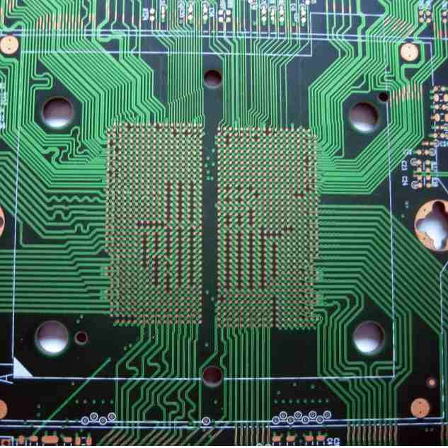
- Denser BGAs may have over 1000 blind vias in the package footprint.
Depth Control
- With blind vias, drilling must stop precisely at the target layer.
- This requires excellent depth control to avoid hitting inner layers.
- Allow for +/- 10% depth tolerance. Adjust annular rings and antipads accordingly.
Filling and Plating
- Blind vias are usually made conductive by electroplating, requiring a seed layer.
- Filling blind vias improves heat dissipation and stability.
- Ensure complete plating penetration into blind via holes.
Via-in-Pad
- Blind vias are often used for inner-layer component pads (via-in-pad).
- This provides a thermal path but can complicate rework.
- Avoid placing blind vias under BGA balls.
Fabricating PCBs with Blind Vias
Fabricating reliable boards with blind vias requires specialized processes and strict quality controls:
Layer Registration
- Drilling blind vias requires precise registration between layers.
- Typical registration tolerance is around 25um (1 mil).
- Laser direct imaging (LDI) improves registration accuracy.
Via Drilling
- Micro-vias require laser drilling, which offers small diameters and depth control.
- Mechanical drilling can potentially be used for larger blind vias.
- A combination of techniques may be needed.
Depth Control
- During drilling, depth must be monitored in real time to end at the target layer.
- Allow for +/- 10% depth tolerance.
- Computerized Z-axis controls provide precision depth drilling.
Plating Processes
- Electroless copper followed by electroplating is used to plate blind via holes.
- Ensure uniform plating thickness on inner layer walls.
- Filling blind vias requires pressure fill processes.
Automated Testing
- Testing vias requires impedance, resistance, and optical inspection.
- Flying probes and x-ray are used to verify blind via quality.
- Automated optical inspection looks for defects and blockages.
Selecting a Fab Partner
- Work with a fabricator experienced in advanced HDI techniques.
- Ensure they can meet the specified PCB tolerances.
- Discuss expected yields and costs. Volume discounts may apply.
Applications Using Blind Vias
Some of the common applications leveraging blind vias:
High Pin Count Packages
- High density interconnects needed under large BGAs, CSPs and flip chip packages.
- Blind and micro-vias provide routing between package pads and inner layers.
IC and Component Vias
- Blind vias allow via-in-pad connections for SOICs, QFNs and other ICs.
- Greatly simplifies routing dense component pads to inner layers.
Multi-Layer Boards
- Advanced PCBs may use 20 layers or more. Blind vias are essential.
- Allows separating circuits and referencing power/ground across layers.
HDI Boards
- Tighter trace/space rules require blind vias for routing capacity.
- Microvias combined with blind vias optimize layer utilization.
RF and High Speed
- Preserve uninterrupted ground planes by routing signals layers with blind vias.
- Avoid stubs and impedance mismatches.
Flex/Rigid PCBs
- Enable selective connections between rigid and flex sections.
- Improve density and flexibility versus through vias.
Questions and Answers on Blind Vias
Here are some common questions related to blind vias in PCB design and fabrication:
Q: What is the typical size range for blind via holes and pads?
A: Blind via holes are typically between 0.1 mm to 0.3 mm in diameter. Landing pads around the holes range from 0.2 mm to 0.5mm. Allow at least 0.1mm annular ring for the pad. Laser drilled vias can have smaller diameters.
Q: How many layers can blind vias practically connect in a multilayer PCB?
A: It’s quite feasible to fabricate blind vias in boards up to 20-30 layers. However, this increases fabrication complexity. As a guideline, limiting blind vias to around 6-8 contiguous layers improves manufacturability and yield.
Q: Does using blind vias increase the cost of PCB fabrication?
A: Yes, the specialized processes add cost versus a simple 2-layer board. However, blind vias enable higher density routing, fewer layers, better performance, and often offset the impact. Discuss expected yields and volume pricing with your fabricator.
Q: Can microvias be combined with blind vias?
A: Yes, blind microvias are very useful in advanced HDI designs. For example, blind laser vias can connect layers 2 and 3 while microvias then connect Layer 3 and Layer 1. This provides maximum routing flexibility.
Q: Is it better to use filled or unfilled blind vias?
A: Filling blind vias has several advantages including better heat dissipation, reduced outgassing, and improved structural integrity. So filled vias are typically preferred, unless cost is the main driver.
Conclusion
Blind vias are a critical tool in designing and fabricating high density, high performance printed circuit boards. By selectively connecting internal layers to outer layers, blind vias enable complex routing, higher component density, rigid-flex integration, and improved signal integrity. However, realizing the benefits of blind vias requires attention to detail in the design, layout, and fabrication processes. When utilized effectively, blind vias facilitate innovative PCB solutions to meet the needs of cutting edge electronics.


Leave a Reply