Introduction
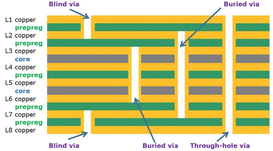
A via is a small opening in a printed circuit board (PCB) that allows different layers to be electrically connected. Vias make it possible to route traces between different layers in the PCB stackup. There are several types of vias used in PCBs, including through hole vias, blind vias, and buried vias. This article will focus on explaining what blind vias and buried vias are, why they are used, and the key differences between them.
What is a Blind Via?
A blind via is a hole that connects one or more internal layers of a PCB without going through the entire board. Blind vias stop at an internal layer and do not penetrate all the way through from the top to the bottom layer.
Key Characteristics of Blind Vias
- Only connect internal layers of a multilayer PCB, not the external layers
- Stop at an internal layer, do not go through entire PCB stackup
- Requires careful laminate and prepreg selection
- Requires specialized drilling equipment
- Can be filled or plated through
Why Use Blind Vias?
There are several reasons why blind vias are used in PCB designs:
- Save space: Blind vias take up less space on the outer layers compared to through hole vias. This allows for higher component densities.
- Improve signal integrity: Blind vias allow signals on inner layers to transition to another layer without having to go through the entire board. This can improve signal quality.
- Simplify routing: Using blind vias between internal layers simplifies trace routing as the connections do not use up space on the outer layers.
- Reduce cost: PCBs with blind vias may have a lower overall cost compared to boards with only through hole vias, depending on the design.
Challenges with Blind Vias
While blind vias offer advantages, they also come with some challenges:
- Limited connectivity: Blind vias can only connect the layers they span, limiting routing options.
- Complex fabrication: Additional steps are required during PCB fabrication to create blind vias, increasing costs.
- Testing difficulties: It can be harder to probe and inspect blind vias during testing compared to through hole vias.
What is a Buried Via?
A buried via is a special type of blind via that does not connect to either the top or bottom outer layer of the PCB. Buried vias are “buried” in between internal layers of the board.
Key Characteristics of Buried Vias
- Connect only internal layers, not the external top or bottom layers
- Fully enclosed within the PCB, no opening on the outer layers
- Requires very careful prepreg and laminate selection
- Challenging to fabricate and inspect
- Can be filled or plated through
Why Use Buried Vias?
There are some specific reasons to use buried vias in a PCB design:
- Maximize layer usage: Buried vias don’t take up space on the outer layers, allowing full use of the external layers.
- Optimize layer transitions: Signals can transition between internal layers without impacting the top or bottom layers.
- Simplify layout: With complex designs, buried vias can simplify PCB layout and routing.
- Improve signal integrity: By keeping signals enclosed internally, buried vias minimize external noise pickup.
- Enable higher density: Buried vias support more dense component placement and routing.
Challenges with Buried Vias
While beneficial in some cases, there are tradeoffs when using buried vias:
- Limited access for probing/testing: Since they are fully buried, it is difficult to physically access buried vias.
- Complex fabrication process: Additional steps are needed to fabricate PCBs with buried vias, increasing costs.
- Specialized materials required: The PCB laminates must be specifically designed to allow creation of buried vias.
- Difficult rework: It can be very challenging to rework or replace buried vias if needed.
Key Differences Between Blind and Buried Vias
Blind vias and buried vias serve different purposes in PCB designs. Here are some of the major differences between the two:
| Blind Via | Buried Via |
|---|---|
| Connects between internal layers and one outer layer | Connects only between internal layers |
| Requires via exit hole on one outer layer | No exit hole on outer layers |
| Simpler fabrication process | Complex fabrication requirements |
| Easier to inspect and probe | Very difficult to access for testing |
| Less impact on material selection | Requires compatible laminate and prepreg |
| Lower cost | Generally higher cost |
When to Use Each Type
- Use blind vias when transitioning between internal layers if an exit hole on an outer layer is acceptable
- Use buried vias when signals must be fully contained internally without any interfacing with top/bottom layers
PCB Fabrication Considerations
Using blind and buried vias in a PCB design adds additional considerations during fabrication and assembly.
Laminaite and Prepreg Materials
The laminate and prepreg materials used in the PCB must be specifically compatible with creating blind and buried vias. The fabrication process requires materials that can be mechanically drilled and laser drilled to create these specialty vias.
Layer Alignment
The PCB layers must be precisely aligned and stacked up to ensure the blind and buried vias properly connect between the correct internal layers.
Via Plating and Filling
Blind and buried vias require plating to create the conductive barrel. Additional steps may be needed to fill vias to create a flat surface. These processes require precision.
Via Routing and Escape Routing
The vias must be routed carefully between layers, with precise escape routing on the correct outer layers for blind vias. Buried vias require no external escape routing.
Testing and Inspection
Testing PCBs with blind/buried vias is more complex. Specialized techniques like x-ray inspection may be necessary to verify internal layer connections.
Rework and Modifications
It is very difficult to rework or modify blind/buried vias if needed, compared to through hole vias. Changes often require complete PCB replacement.
Applications and Examples

Some examples of where blind and buried vias are used in PCBs:
- High density interconnect (HDI) PCBs
- High pin count BGA packages
- Flip chip and wafer level packaging
- Multilayer RF/microwave PCBs
- LED lighting PCBs
- Automotive electronics boards
- Advanced telecommunications products
Specific applications like power planes, signal routing, and RF transitions can benefit from using blind and buried vias. They enable complex internal connections without consuming outer layer space.
Pros and Cons of Using Blind and Buried Vias
Pros
- Save space on external layers
- Simplify routing on outer layers
- Improve signal quality by isolating layers
- Allow higher component densities
- Enable greater PCB miniaturization
Cons
- Limited connectivity between layers
- More complex PCB fabrication process
- Requires advanced drill/laser technology
- Difficult to probe and inspect internally
- Repair and rework is very challenging
- Generally increases cost over through hole vias
Blind and Buried Vias in HDI PCBs
High Density Interconnect (HDI) PCBs frequently utilize blind and buried vias to achieve denser connections:
- Tight component spacing requires short connections between layers
- Blind vias allow connections from inner to outer layers
- Buried vias connect inner layers without using outer space
- Laser drilling can create microvias to connect HDI layers
Blind/buried vias help maximize routing density by avoiding the outer layers. Microvias formed with laser drilling provide precision interconnections. This enables greater miniaturization and component density.
Summary
- Blind vias connect internal PCB layers without passing through the full board stackup
- Buried vias are encapsulated fully within inner board layers
- Blind/buried vias save space on outer layers and simplify routing
- More complex fabrication is required to produce blind/buried vias
- These specialty vias enable higher component density and miniaturization
- HDI PCBs leverage blind/buried vias to maximize interconnect density
Using the right types of vias in a PCB design provides flexibility to route complex connections and optimize board layout. Both blind and buried vias have specific advantages for multilayer boards requiring dense component placement and routing.
Frequently Asked Questions
What are some key benefits of using blind vias?
Some benefits of using blind vias include:
- Saving space on external PCB layers
- Simplifying routing by reducing congestion on outer layers
- Allowing higher component and interconnect densities
- Improving signal integrity by isolating layers
- Reducing EMI/noise issues by containing signals internally
When is it better to use buried vias versus blind vias?
Use buried vias when signals and connections must be completely contained between inner PCB layers. Buried vias do not connect to either the top or bottom external layers. Blind vias are preferable when a connection to one of the outer layers is needed.
What are the main fabrication challenges with blind and buried vias?
Fabricating blind and buried vias requires advanced drilling/laser technology and very precise layer-to-layer alignment. The PCB materials must also be specifically compatible. Testing and reworking blind/buried vias is more difficult compared to through hole vias. The specialized processes increase overall fabrication costs.
How are blind/buried vias created?
Blind and buried vias are created by using mechanical drilling and/or laser drilling. Mechanical drills bore partially through the PCB layers, while laser drilling provides precision microvias. The vias are then plated to connect the layers. Additional filling may be performed.
Can buried vias be implemented in 2-layer PCBs?
No, buried vias can only be implemented in multilayer PCBs with 4 or more layers. Buried vias require at least two fully encapsulated inner layers to be buried between. 2-layer boards only have the external top and bottom layers.


Leave a Reply