Introduction
In printed circuit board (PCB) design, blind vias play an important role in allowing connections between different layers of the board while conserving space. Blind vias are plated-through holes that connect only two or more internal layers of a PCB without connecting to the external layers.
One of the most critical factors to consider when working with blind vias is the aspect ratio – the ratio between the via diameter and the finished via depth. The aspect ratio can have significant impacts on the manufacturability and reliability of blind vias during PCB fabrication and assembly.
In this article, we will examine blind via aspect ratios in depth, including:
- What is a blind via aspect ratio and why does it matter?
- Recommended blind via aspect ratios
- Consequences of having a high aspect ratio
- How to design blind vias with optimal aspect ratios
- Strategies for high aspect ratio blind vias
- Impact of aspect ratio on PCB cost
Properly designing blind vias with the right aspect ratio is essential for creating durable and defect-free circuit boards. Let’s dive in and explore the key considerations around blind via aspect ratios in PCB design.
What is a Blind Via Aspect Ratio and Why Does it Matter?
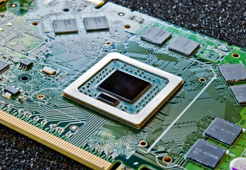
The blind via aspect ratio refers to the relationship between the diameter of the blind via hole and the thickness of the PCB from the bottom of the blind via to the next layer. It is calculated by dividing the finished blind via depth by the target hole diameter.
For example, if a blind via connecting layers 3 and 5 of a PCB has a finished depth of 200 microns, and the drill diameter is 100 microns, then the aspect ratio would be 2:1.
The blind via aspect ratio is important because it affects:
- Manufacturability: A higher aspect ratio makes the blind via more difficult and expensive to fabricate. There are limits to how high an aspect ratio most PCB manufacturers can achieve.
- Reliability: Blind vias with too high of an aspect ratio are prone to problems like reduced hole wall adhesion, uneven plating thickness, and cracking under thermal and mechanical stresses.
- Assembly: It becomes harder to completely fill high aspect ratio blind vias, resulting in potential voids and decreased solder joint reliability.
Ideally, you want an aspect ratio that balances manufacturability, reliability, and assembly requirements. Let’s look at what the recommended ratios are.
Recommended Blind Via Aspect Ratios
There are some general guidelines around optimal blind via aspect ratios:
- 1:1 is ideal and preferred if possible. This balances manufacturability and reliability.
- Up to 2:1 is generally acceptable for most board shops. Process control and plating quality become more critical above 2:1.
- 2:1 to 4:1 is possible but requires more stringent process controls, equipment capabilities, and potential additional costs. It also becomes harder to reliably fill the vias during assembly above 2:1.
- Over 4:1 is not recommended and should be avoided if possible. Very few PCB fabricators can reliably produce blind vias over 4:1. The reliability risks also increase considerably.
Here is a quick reference table for recommended maximum blind via aspect ratios:
| Aspect Ratio | Rating |
|---|---|
| 1:1 | Ideal |
| Up to 2:1 | Acceptable |
| 2:1 to 4:1 | Possible but not preferred |
| Over 4:1 | Avoid if possible |
Of course, you should always consult with your PCB manufacturer on their specific capabilities and process limitations as well. But in general, try to design your blind vias to be 1:1 to 2:1 whenever possible.
Consequences of Having a High Aspect Ratio
When blind vias have too high of an aspect ratio, you risk running into several manufacturability and reliability issues, including:
- Plating voids: It becomes increasingly difficult to achieve conformal plating along the full depth of the via. This can lead to cracks or missing plating.
- Reduced adhesion: The plating adhesion to the via barrel decreases with higher aspect ratios, which can ultimately lead to plating separation and open circuits.
- Etching challenges: Higher aspect ratios make it harder to cleanly etch the via hole without leaving residue.
- Stress cracking: Thermal and mechanical stresses concentrate at the weaker plated areas of high aspect ratio vias, leading to cracking over time.
- Assembly voids: It becomes very difficult to completely fill ultra-high aspect ratio vias with solder or epoxy. This can create voids leading to joint failure.
- Lower production yields: Due to the above issues, fabricators usually see more defects and lower yields when producing boards with excessive blind via ratios.
To avoid these types of problems, keep your blind via aspect ratios within recommended limits and avoid going over 4:1 whenever possible. Work with your PCB manufacturer to understand their capabilities.
How to Design Blind Vias with Optimal Aspect Ratios
Here are some tips to help design blind vias with optimal aspect ratios:
1. Plan layer stack-up accordingly
- Minimize thicknesses between layers needing blind via connections to limit depth.
- Arrange signal layers needing interconnections close together.
- Place ground/power planes in between layers with blind vias.
2. Follow size requirements
- Keep drill diameter above 0.2mm (8 mil) minimum to enable plating.
- Use larger diameters for longer blind vias to improve aspect ratio.
3. Consult manufacturer design rules
- Ask your fabricator about their specific aspect ratio limits and minimum drill sizes.
- Design your blind vias within their guidelines.
4. Perform design rule checking
- Run DRC in your PCB design software to automatically flag any excessively high aspect ratios.
- Manually inspect and confirm aspect ratios as well.
5. Prototype and cross-section
- Prototype a few boards to test plating quality and inspect cross-sections.
- Tweak design as needed to improve reliability before full production.
Paying attention to these tips when laying out your PCB will help ensure your blind vias have optimal aspect ratios for manufacturing and long-term performance.
Strategies for High Aspect Ratio Blind Vias
For cases where you cannot avoid using some blind vias with high (3:1 to 5:1) aspect ratios, here are some strategies to improve their manufacturability and reliability:
- Increase via diameters where possible to bring down aspect ratio. But be aware this uses more space.
- Use thicker finished copper plating like 20μm to improve plating quality and strength.
- Implement skip plating on deeper non-critical vias to reduce plating thickness.
- Require stringent etch process controls at the PCB fab to prevent etching issues.
- Request additional via wall conditioning like plasma treatment to increase plating adhesion.
- Require 100% plating inspection using cross-sectioning or x-ray imaging.
- Consider HDI processes which can better handle high aspect ratio blind vias. But this often comes with higher costs.
- Avoid placing high value components by any critical or high aspect ratio vias to minimize impact of any failures.
- Perform extensive reliability testing like thermal shock, temperature cycling, and vibration testing.
While not ideal, using combinations of these strategies can make very high aspect ratio blind vias more viable when there are no other design options.
Impact of Aspect Ratio on PCB Cost
Blind via aspect ratios also affect the fabrication costs for your PCBs:
- In general, going above 2:1 aspect ratios will increase cost due to requiring more advanced and tightly controlled processes.
- Going above 4:1 may incur additional charges or require shifting to more expensive HDI board processes.
- Any reliability testing or additional process steps needed for high aspect ratio vias also add cost.
- However, using new laser drilling techniques can help reduce fabrication costs for high aspect ratio vias vs traditional mechanical drilling.
To get accurate pricing information, always check with your PCB manufacturer and get quotes for your specific design rather than just relying on their standard published costs. The number of high aspect ratio blind vias and their characteristics will factor into the final board pricing.
Conclusion
Blind via aspect ratio is a crucial parameter that must be carefully considered when designing PCBs. Following recommended guidelines around via diameter and depth will ensure optimal manufacturability, reliability, and cost. Shooting for 1:1 to 2:1 aspect ratios is ideal. Going above 4:1 is not recommended and comes with significant risks. A properly designed layer stack-up is critical to facilitating blind vias with acceptable aspect ratios. When ultra-high aspect ratios cannot be avoided, steps must be taken to mitigate risks and test thoroughly before production. With upfront planning, designers can implement blind vias in their PCBs that balance performance, yield, and fabrication cost.
Frequently Asked Questions
What are some typical PCB layer stack-ups to optimize blind via aspect ratios?
Some typical layer stack-up strategies include:
- Placing signal layers that need interconnects next to each other to minimize blind via depth.
- Putting ground or power planes in between signal layers needing blind vias.
- Locating high-speed signals on layers closer to the PCB surface rather than buried deep, which would require unnecessarily long blind vias.
How does skip plating help for high aspect ratio blind vias?
Skip plating involves leaving a section of the blind via unplated near the bottom. This reduces the plated thickness along the via length, improving plating uniformity deeper in the hole. It also decreases stresses. But skip plating may only be used for non-critical vias like grounds.
Can multiple smaller diameter blind vias be used instead of one larger one?
Yes, using multiple smaller blind vias to connect two layers can help reduce individual aspect ratios versus one larger via. However, this takes up more board space. The size and number should be considered carefully based on current requirements.
How does HDI PCB fabrication help with high aspect ratio blind vias?
HDI allows for much thinner dielectric layers, smaller via diameters, and tighter process controls. This enables reliable fabrication of blind vias up to 10:1 aspect ratios. HDI is more expensive though. It is not suitable for all designs or production volumes.
Does laser drilling enable higher aspect ratio blind vias versus mechanical drilling?
Yes, newer laser drilling methods can produce extremely straight blind via holes with very high aspect ratios exceeding 8:1. This can help reduce fabrication costs. However, laser drilling has limitations on hole diameters and board materials.
Leave a Reply