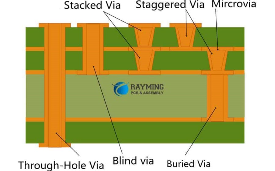
Printed circuit boards (PCBs) use vias to create connections between different layers of the board. Vias come in several types, with two of the most common being blind vias and buried vias. Understanding the differences between these via types and when to use each one is important for PCB designers.
What is a Via?
A via is a plated through hole that connects two or more layers in a PCB. Vias create vertical interconnections between layers, allowing signals to travel between layers of the board. The key features of a standard through hole via are:
- Connects two or more layers of a PCB
- Fully plated along the entire length of the hole
- Extends through the entire PCB from top to bottom
Standard through hole vias are the most basic type of via used in PCBs. However, more complex boards often require different types of vias, such as blind and buried vias.
What is a Blind Via?
A blind via is a vertical interconnect that connects one or more internal layers of a PCB without going all the way through the board. The key features of blind vias are:
- Connects internal layers without reaching the top or bottom layer
- Often used on high density boards
- Allows flexibility in routing between internal layers
- Requires additional drilling steps
Blind vias are fully plated but do not extend to the outermost layers of the PCB. They create selective connections between internal layers that don’t require accessing the top or bottom layer. Blind vias are often used for high density designs where routing space is limited.
Here is a cross-section diagram of a blind via:<table> <tr> <th>Layer 1 (Top layer)</th> <th></th> </tr> <tr> <td>Layer 2</td> <td>Blind Via</td> </tr> <tr> <td>Layer 3</td> <td></td> </tr> <tr> <td>Layer 4</td> <td></td> </tr> <tr> <td>Layer 5 (Bottom Layer)</td> <td></td> </tr> </table>
Advantages of Blind Vias
- Allow connections between internal layers without using outer layers
- Help minimize layer transitions
- Enable higher routing density compared to through vias
- Allow splitting power and ground planes while maintaining connections
Disadvantages of Blind Vias
- Require additional drilling steps
- More complex and expensive manufacturing process
- Require planning ahead in layout to place exit points on inner layers
What is a Buried Via?
A buried via is a plated through hole that connects two or more internal layers of a PCB without connecting to the outer top or bottom layers. The key features are:
- Connects only internal layers
- Does not extend to either outer layer
- Fully plated along hole length
- Often used to minimize layer transitions
Buried vias create connections between internal layers while remaining buried in the middle of the PCB. They do not make contact with either the top or bottom layer. Buried vias help optimize routing density and minimize the use of outer layers.
Here is a diagram of a buried via:<table> <tr> <th>Layer 1 (Top layer)</th> <th></th> </tr> <tr> <td>Layer 2</td> <td>Buried Via</td> </tr> <tr> <td>Layer 3</td> <td></td> </tr> <tr> <td>Layer 4</td> <td></td> </tr> <tr> <td>Layer 5 (Bottom Layer)</td> <td></td> </tr> </table>
Advantages of Buried Vias
- Minimizes use of outer layers for internal connections
- Increases routing density compared to blind vias
- Allows splitting power and ground planes while maintaining connections
- Reduces layer transitions and improves signal integrity
Disadvantages of Buried Vias
- Require complex and expensive manufacturing process
- Adds steps to PCB fabrication process
- Requires planning ahead in layout stages
- Repairs and rework are more challenging
Blind Via vs. Buried Via
Blind vias and buried vias share some similarities, but also have key differences:<table> <tr> <th></th> <th>Blind Via</th> <th>Buried Via</th> </tr> <tr> <td>Connects Outer Layers</td> <td>No</td> <td>No</td> </tr> <tr> <td>Connects Inner Layers</td> <td>Yes</td> <td>Yes</td> </tr> <tr> <td>Fully Plated</td> <td>Yes</td> <td>Yes</td> </tr> <tr> <td>Manufacturing Complexity</td> <td>Moderate</td> <td>High</td> </tr> <tr> <td>Repair Complexity</td> <td>Moderate</td> <td>High</td> </tr> </table>
Some key differences:
- Blind vias connect one or more inner layers and one outer layer. Buried vias only connect inner layers.
- Buried vias are more complex and expensive to manufacture than blind vias.
- Blind vias are easier to repair and rework compared to buried vias.
When to Use Each Type
Here are some guidelines on when to use each type of via in a PCB design:
Use blind vias when:
- You need connections between inner layers and only one outer layer
- Design has moderate layer count and density
- Somewhat complex layout but easy repair ability needed
Use buried vias when:
- Connections are only needed between inner layers
- Design has high layer count and density
- Maximizing routing density is critical
- Performance needs to be optimized
Use through vias when:
- Connections between many layers are required
- Board has lower complexity and density
- Easier manufacturing and repair is preferred
Design Considerations
Here are some important considerations when working with blind and buried vias in your designs:
- Plan layouts ahead of time to locate exit points for blind/buried vias.
- Minimize the use of vias when possible to optimize manufacturability.
- Follow stackup guidelines from your manufacturer.
- Be aware of any special DRC rules for blind/buried vias.
- Consider any impedance matching needs for sensitive signals.
- Weigh costs vs. benefits when choosing via types.
- Account for limitations on the number of blind/buried vias.
Careful planning is key to effectively implementing blind and buried vias. Work closely with your PCB manufacturer to understand capabilities and limitations.
Summary
- Blind vias connect inner layers without reaching top or bottom layers. Buried vias connect only inner layers.
- Blind vias offer easier manufacturability and repair than buried vias.
- Buried vias enable maximum routing density but increase complexity.
- Choose via type based on layer count, density, performance needs and cost considerations.
- Plan layouts ahead of time and work closely with manufacturers.
Frequently Asked Questions
What are some examples of when to use blind vias?
Some examples of good uses for blind vias:
- Connecting a power plane in an inner layer to an outer layer for power distribution.
- Creating selective connections between inner layer signals without using outer layers.
- Optimizing routing density on moderate complexity designs.
- Avoiding transitions through multiple layers for high speed signals.
How do blind vias impact the manufacturing process?
Blind vias require additional drilling steps to create the holes that do not go through the entire board. This adds some time and cost versus a standard through hole via. However, blind vias are not as complex to manufacture as buried vias since they connect to one of the outer layers.
Is there a limit to the number of blind or buried vias I can use?
There are typically restrictions on the maximum number of blind/buried vias from a manufacturability standpoint. This limit depends on several factors like board thickness, hole size, and capability of the fabricator. Check with your board manufacturer for their specific limitations.
What are the main reliability risks with buried vias?
Buried vias have higher reliability risks than blind vias. Some key risks are:
- Improper plating of via holes during manufacturing.
- Voids or cracks within the plated barrel of the hole.
- Separation of inner layer connections over time.
- Damage from heat exposure.
Careful process controls and testing helps minimize buried via reliability issues.
How can I repair a buried via if needed?
Repairing buried vias is very difficult compared to blind or through vias. Often the entire PCB must be disassembled or scrapped in order to access and replace a buried via. Some options like epoxy injection or conductive ink filling may be possible but have limitations. Avoiding buried vias when possible is recommended if easy repair is necessary.


Leave a Reply