Blind holes, also known as buried vias, are an essential component in printed circuit board (PCB) design. As electronics become more complex and compact, the use of blind vias helps connect different layers efficiently without using up valuable surface space. This article will provide a comprehensive overview of blind hole PCBs, their function and design considerations.
What are Blind Hole Vias?
A blind via is a hole that connects two or more layers of a PCB without going all the way through the entire board. It creates an electrical connection between internal layers that is invisible from the surface.
Blind vias are categorised into three types:
- Blind Via: Connects an outer layer to one or more inner layers but does not extend to the other outer layer.
- Buried Via: Connects two or more inner layers only. Does not connect to either outer layer.
- Micro Via: A blind via with a diameter less than 150 μm (0.006″). Used in high-density PCBs.
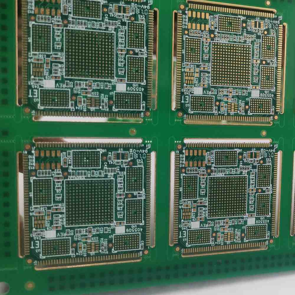
Fig.1 – Different types of blind hole vias
The key advantages of using blind vias include:
- Save space on outer layers for more trace routing.
- Allow connections between non-adjacent layers.
- Reduce overall hole drilling.
- Improve signal integrity for high-speed designs.
- Enable greater routing flexibility.
Why Use Blind Vias?
Here are some of the main reasons blind and buried vias are used in PCBs:
Optimizing Layout Space
By putting vias between layers and keeping routing internal, valuable space is freed up on the external layers for more complex routing. This enables greater design flexibility and miniaturization.
Connecting Non-Adjacent Layers
Blind vias allow connections between non-adjacent layers, something not possible with through-hole vias. For example, connecting the top layer to an internal power or ground plane deeper in the stackup.
High Density Interconnects
Microvias help maximize PCB density. Their small size (< 0.15mm) allows many more connections in the same area versus standard vias. High density blind/buried vias are key in advanced HDI (High Density Interconnect) boards.
Signal Integrity
For high-speed digital circuits, blind/buried vias isolate sensitive signals between layers. This shields them from noise on outer layers and provides a continuous return path to the ground plane. Better SI performance overall.
Improved Manufacturability
Blind vias require less drilling compared to through-hole vias, reducing stress on PCB fabrication equipment. They also allow designers to optimize layer stackups for ease of manufacturing.
Routing Flexibility
Blind vias open up routing options, like routing a section of a track internally then bringing it out on a different layer. Through-hole vias mandate entering and exiting on the same set of layers.
Lower Cost
Requiring less drilling, blind vias use less materials during fabrication. They also take up less space, allowing smaller PCBs overall and more boards per panel further reducing costs.
How Blind Vias are Constructed

There are a few techniques used to create the blind via hole during PCB fabrication:
Laser Drilling
A laser is used to selectively ablate (vaporize) the laminate layers to form a blind via. Precise depth control allows drilling to stop at any inner layer. Works well for microvias due to the small spot size.
Plasma Etching
Similar to laser but uses plasma to etch away the blind hole. Not as common as laser drilling.
Controlled Depth Mechanical Drilling
A mechanical drill bit penetrates to a preset depth to create the blind hole. Depth is controlled by the drill feed rate and speed. Low cost process good for large vias (>0.4mm) but not for microvias.
Photo Process
A photosensitive dielectric layer is imaged to selectively create the blind via in the desired location. Subsequent plating builds up the blind hole barrel. Allows very high density small vias.
Once the hole is formed, the blind via is plated (coated) with copper to form the conductive barrel surface just like a through-hole via. This connects the layers together electrically.
Blind and Buried Via Design Rules
There are some key design rules to follow when working with blind/buried vias:
- Via Annular Ring: This is the clearance between the via barrel and adjacent copper pads or traces. Annular ring must be wide enough to allow forregistration tolerancesduring drilling and prevent shorts.
- Minimum Via Size: Determined by capabilities of the drilling method used. Laser drilled microvias can be 0.1mm or smaller. Mechanically drilled blind vias typically >0.3mm.
- Spacing/Density: Blind vias require minimum spacing between adjacent vias. Limits on maximum via density must be followed.
- Depth Registration Accuracy: Drilling accuracy affects layer-to-layer alignment. More restrictive depth tolerance required as blind depths get shorter.
- Aspect Ratio: The ratio of via drill depth to its diameter. This is limited to avoid reliability issues like poor plating adhesion.
Fig.2 – Key blind via design rules
Always check your PCB manufacturer’s specific capabilities and design rules for blind and buried vias to ensure manufacturability.
Blind Via Reliability Factors
For a robust design, blind vias must be reliable over the product lifetime. Here are some key factors:
- Plating Quality: Full circumferential plating coverage inside the blind hole is critical. Voids can cause opens.
- Barrel Resistance: Copper plating must provide low resistance current path between layers. Thin or lossy platings increase impedance.
- Registration Accuracy: Tight depth control needed for blind depths.Variation cancause shorts between layers.
- Pad/Trace Adhesion: Environmental stress can cause traces or pads to delaminate around vias. Thermal cycling is a major stressor.
- Outgassing: Trapped air in the blind hole can be problematic. It gets pressurized during reflow soldering and escapes by delaminating the plating interfaces.
Proper design, layout considerations, and manufacturing process controls help mitigate these reliability risks.
Modeling and Simulation
Blind vias affect signal and power integrity which must be assessed during design. Key parameters to model include:
- Via Impedance: Resistance and inductance of the via barrel impacts transmission line impedance.
- Cross-Talk: Noise coupling between closely spaced vias should be simulated.
- Reflections: An impedance discontinuity at the blind via can cause signal reflections.
- Power Drop: Current through a blind power via has inherent voltage drop that affects power distribution.
Various PCB modeling tools like Ansys SIwave, Mentor HyperLynx, and Cadence Sigrity PowerDC can simulate blind vias to gauge their performance prior to fabrication.
Layout Best Practices
Proper layout technique is vital to maximizing the performance of blind vias while mitigating reliability risks:
- Place vias to minimize overall drilling. Share vias between nodes if possible.
- Group vias together into “via farms” then route connections to minimize stubs.
- Use thermals to reduce drilling-related stress on plated through hole (PTH) pads.
- Place test points on inner layers to verify blind via connectivity.
- Keepouts around the via perimeter ensure space for annular ring.
- Apply soldermask webing between dense vias to reduce solder wicking.
- Minimize unused sections of blind segments in layout to reduce risk of trapped air pockets during lamination.
Fig.3 – Example layout practices for blind vias
Applications of Blind Vias
Some examples of where blind vias provide design advantages:
High Pin Count BGAs
The tight pin pattern requires multiple layers to escape the dense array. Blind and microvias route signals internally between layers.
LED Printed Circuit Boards
LED PCBs need many layers to manage thermal dissipation. Blind vias connect the top LED circuitry layer to inner thermal layers without congesting the surface.
RF/Microwave PCBs
Sensitive RF traces are routed internally, shielding them from surface noise. Components can be bottom mounted but still connected to the RF layer using blind vias.
High Speed Digital
Blind vias containing fast logic signals should connect to a reference plane directly underneath to minimize stubs.
Multi-Layer Boards
Complex boards with 8+ layers rely heavily on blind and buried vias to route between non-adjacent inner layers since through-hole vias only connect adjacent layers.
Blind and Buried Via Cost
Blind via PCBs typically cost more than simple 2-4 layer boards with just through-hole vias due to:
- Additional drilling to create blind depths.
- More complex layer stackup alignment.
- Tighter process controls on plating quality and drilling accuracy.
- Potentially lower panel utilization if via density is very high.
However, blind vias enable reduced overall board sizes, fewer drill holes, better performance, and higher routing capability. These benefits usually offset the marginally higher costs compared to a simpler PCB design.
Consulting your fabricator on costs, capabilities, and lead times for blind vias during design is recommended.
Frequently Asked Questions
Here are some common FAQs related to working with blind vias:
What is the typical size range for blind vias?
Blind vias span a wide range from microvias (~0.1mm) to large blind holes >1.0mm. Typical size range is 0.2mm to 0.5mm. Laser drilled microvias down to 0.05mm are possible.
Can a PTH pad connect to a blind via?
Yes, it is common for a PTH component lead to be connected to an internal layer via a blind via. The pad is on the surface while the via connects to the inner layer.
What are thermal relief connections in vias?
Thermal reliefs are small gaps in the connection between pads/traces and plated through holes. This reduces mechanical stress from drilling and heating.
Can a blind via connect a top layer trace that extends across the entire board?
It is possible but not ideal since any registration error could cause a short. A buried via is better for connecting traces that run across the board edge-to-edge.
How are blind vias tested for connectivity?
Test points on inner layers provide a way to probe blind vias. Automated optical inspection and x-ray are used during fabrication to verify plating quality inside blind holes.
Conclusion
Blind and buried vias enable complex, dense PCB designs by efficiently using routing channels between layers. By keeping interconnections internal, they help optimize board space utilization, signal performance, and manufacturability. With careful layout consideration for the design rules and reliability factors, engineers can utilize blind vias effectively while mitigating risks. For advanced PCB technologies expected to dominate future electronics, an understanding of blind hole vias is becoming mandatory knowledge.


Leave a Reply