Introduction
Printed circuit boards (PCBs) are essential components of nearly all modern electronic devices, serving to mechanically support and electrically connect electronic components. As electronic products continue to be designed smaller and with greater functionality, PCBs have evolved to accommodate more complex circuitry and components in increasingly compact spaces. This has led to the widespread adoption of blind and buried vias in PCB manufacturing.
Blind vias and buried vias refer to plated-through holes in a PCB that connect different layers without being visible or accessible from the outer surfaces. These via structures allow connections between internal layers, facilitating high-density interconnects and enabling greater routing flexibility for complex multi-layer boards. In particular, buried vias that are completely concealed within the PCB laminations have become critical enablers for sophisticated designs.
What are Blind Buried Vias?
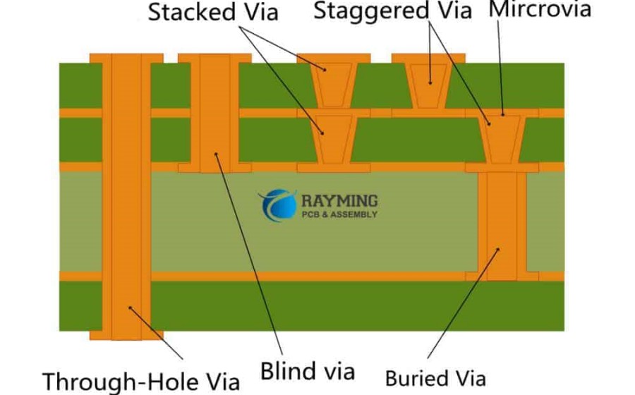
A blind buried via (BBV) combines features of both blind vias and buried vias. Blind vias originate on an external PCB layer and terminate on one or more internal layers. In contrast, buried vias are contained entirely within the internal layers. BBVs connect one or more internal PCB layers to each other without reaching the outer surfaces.<p></p>
Show Image<p></p> <p>Figure 1. Cross-section of a PCB with blind buried vias connecting internal layers.</p>
BBVs provide vertical interconnects between internal layers that avoid breaching the outer surfaces. This is important for high layer-count boards since it allows greater routing flexibility without sacrificing surface area for via landings. The fabrication process and reliability considerations around BBVs also differ from simpler via types.
Benefits of Using Blind Buried Vias
Using BBVs provides several key advantages for complex, dense PCB designs:
Increased Wiring Capacity
By keeping interconnections between internal layers fully contained, BBVs reduce the demand for surface routing channels and via landings. This frees up valuable real estate on the outer layers for placing more surface mount components and routing critical signals. The routing congestion relief enables higher wiring density overall.
Signal Integrity
With blind and buried vias, critical signals can take shorter vertical paths through the board layers, minimizing parasitic inductance compared to routing horizontally across the surface. This allows higher speed signals with reduced interference. BBVs avoid surface exits altogether for contained routes, providing optimal signal integrity.
Reduced Layer Count
The availability of BBVs reduces the number of layers required to route complex designs by offering vertical connectivity for internal signals. This lowers costs and improves manufacturability compared to alternatives using more layers without blind/buried vias.
Design Flexibility
Blind and buried vias enable connections that would otherwise require longer, more convoluted routing paths. This gives designers greater leeway in floorplanning IC and component placement while still meeting all electrical connectivity requirements. BBVs essentially provide a third routing dimension.
Improved Manufacturability
BBVs avoid stub connections which cause reflections and signal quality issues. This makes the finished boards more conducive to high-volume manufacturing and assembly processes. BBVs also allow automated optical inspection since all layers are accessible.
High-Frequency Performance
At microwave and mmWave frequencies, vertical interconnections become critical for managing transmission line effects. BBVs provide contained RF paths between layers for reduced losses, cross-talk, and electromagnetic interference. High frequency or high speed mixed signal designs benefit greatly from incorporating BBVs.
Construction of Blind Buried Vias

Fabricating boards with BBVs requires careful planning, preparation, and control through the multilayer construction process:
1. Define BBVs in Layout
All buried and blind vias are identified clearly in the PCB layout. This includes the layers to be connected, diameter based on current needs, pad shapes, and landed patterns. Layout software assists by defining interconnect rules and design clearances.
2. Select Materials
The laminate materials must exhibit good flow during press cycles to completely fill BBVs. Many advanced dielectric materials are engineered specifically to support HDI techniques. Prepregs may also be specified based on resin content and viscosity.
3. Surface Preparation
Surfaces must be thoroughly cleaned before lamination to allow strong adhesion throughout the layer stackup. Any residual processing chemicals or debris can prevent adequate bonding. Plasma etching is commonly used for surface preparation.
4. Alignment
Careful alignment during layup is critical to achieve interconnections between layers. Laser drilled fiducials provide alignment guides. Maintaining process consistency also improves alignments through the layer stack.
5. Lamination
Applying heat and pressure causes the resin to flow and fills any blind or buried features. The lamination process may require baking steps before curing to prevent voids within plated holes. Fully cured boards then proceed to drilling.
6. Laser Drilling
CO2 or UV laser systems drill all blind and buried vias to connect the predefined layers. High accuracy (±0.002”) is needed to locate buried targets. Plasma cleaning follows to remove debris before plating.
7. Plating
Electroless copper with electrolytic copper plating is used to metalize the laser drilled holes, depositing conductive material onto the interior barrel surfaces. A photolithographic plating resist limits deposition to only desired areas.
8. Stackup Assembly
After all layers are completed individually, they are precisely aligned and laminated together into the final multilayer board. The assembly process depends on maintaining drilled hole locations.
9. Testing
Electrical testing and x-ray inspection validates continuity through buried interconnects. Automated optical inspection also checks capture pads and solder mask coverages on outer layers.
Key Process Considerations
Fabricating reliable BBVs requires careful process engineering and controls:
- Via stubbing – Partial drilling of BBV barrels from outer layers helps locate targets and prevents misalignment. The stubs are etched away after plating.
- Resin control – Matching coefficients of thermal expansion between cured resin and reinforcement is critical to prevent delamination or cracking.
- Surface preparation – Thorough desmearing and oxide treatment improves adhesiveness and wetting into drilled holes during lamination steps.
- Aspect ratios – Higher aspect ratios increase risks of hole wall pullaway and plating voids. Wider BBV pads help minimize this.
- Pad design – Sufficient annular rings around BBV pads prevent wicking failure, especially important for soldered components.
- Lamination – Applying the minimum pressure needed prevents excessive resin squeeze-out from laminations.
- Plating coverage – Uniform plating thickness on hole walls requires properly balanced chemical baths. Full coverage avoids opens.
- Alignment – Maintaining layer-to-layer registration accuracy throughout a multilayer build avoids misaligned or unreliable buried interconnects.
Reliability Considerations
While BBVs provide significant benefits, they also introduce reliability risks that require mitigation:
Voids – Imperfect filling of BBV holes with resin during lamination can lead to plating voids. These gaps in plated barrels cause opens. Careful process controls and x-ray inspection help prevent them.
Separation – Any delamination between layers risks breaking buried interconnects, causing electrical opens. Thorough surface preparation promotes strong adhesion. Shock/vibe testing also checks for potential separation issues.
Thermal stress – CTE mismatches between copper and laminate materials can induce stresses during thermal excursions. This can deteriorate interfaces over time and cause intermittent buried connections.
Moisture – Absorbed moisture in multi-layer boards expands when heated during soldering or assembly, putting mechanical stress on plated barrels. Baking prior to assembly helps drive out moisture.
Fatigue – Thermal cycling and vibrations can fatigue copper interfaces in plated holes over time due to shear forces, potentially forming micro-fractures or cracks.
Applications Using Blind Buried Vias
A few examples of advanced products using HDI PCBs with BBVs include:
- High layer count communication and network switches
- Servers and data storage systems
- Mobile devices – smartphones, tablets, wearables
- Displays and monitors
- Set-top boxes and media players
- Automotive infotainment and ADAS systems
- Aerospace / avionics control systems
- Medical imaging systems
As electronic devices continue trending toward light weight, small size, high speed, and complexity, blind and buried vias enable this evolution by supporting ever greater functionality and component densities. BBVs alleviate routing congestion and provide electrical performance benefits essential for many emerging applications. With rigorous design and manufacturing processes, they can be implemented reliably into the most challenging multilayer circuits.
Key Points Summary
- Blind buried vias connect internal PCB layers without breaching outer surfaces
- Help maximize routing density by reducing demand for surface traces/lands
- Enable high-speed signal paths with minimal parasitics
- Reduce overall layer counts versus routing everything horizontally
- Provide design flexibility for efficient floorplans and placements
- Are fabricated using controlled lamination, laser drilling, and plating
- Require strict process controls to ensure quality buried interconnects
- Mitigate risks like plating voids, delamination, thermal stresses
- Are widely used in advanced electronics across many industries
FAQ
Here are answers to some frequently asked questions about blind buried vias:
What are the main disadvantages of using blind buried vias?
The fabrication process for boards with BBVs is more complex and requires tighter tolerances and process controls. This can lead to lower yields and higher costs compared to standard multilayer boards. Testing for reliability of buried interconnects is also more challenging.
What are some typical blind buried via dimensions?
BBV hole diameters commonly range from 0.003″ to 0.015″ while anti-pad diameters vary from 0.006″ to 0.020” depending on circuit current needs. Aspect ratios typically run from 3:1 to 10:1.
Can microvias be blind and/or buried?
Yes, microvias with diameters below 0.005” can definitely be implemented as blind and/or buried interconnects between layers. This further expands routing capacity. However, the fabrication challenges are greater at smaller scales.
How many blind buried vias can be accommodated in a PCB?
This depends on the board layer count, densities, and layout complexity. In practice, there is no hard limit, but thousands to tens of thousands of BBVs can be incorporated on higher layer count boards.
Are there alternative solutions to blind/buried vias?
Yes, newer interlayer interconnect technologies are emerging such as stacked microvias or conductive ink vias. However, BBVs remain the most widely adopted and cost-effective solution for HDI when appropriately designed and manufactured.


Leave a Reply