Introduction
In printed circuit board (PCB) design, vias are plated through holes that provide electrical connections between layers in the board. Vias come in several types, including blind, buried, and through-hole vias. Blind and buried vias are important for high-density interconnects in multilayer PCBs.
In this article, we will discuss what blind and buried vias are, their benefits, design considerations, and how to implement them effectively in your PCB layouts.
What are Blind and Buried Vias?
Blind Vias
A blind via is a hole that connects one layer to another layer, but does not go through the entire PCB stackup. Blind vias connect an outer layer to one or more inner layers, but do not extend to the opposite outer layer.
For example, in an 8-layer board, a blind via could connect Layer 1 to Layer 5, without connecting all the way through to Layer 8. Blind vias are often used to route high-density BGAs and other components with interconnects between non-adjacent layers.
Buried Vias
A buried via connects two or more inner layers in a PCB, but does not connect to either outer layer. Buried vias are completely internal to the board.
For instance, in a 6-layer board, a buried via could join Layer 3 to Layer 4, without connecting to Layer 1 or Layer 6. Buried vias help optimize routing density for internal signals.
Benefits of Using Blind and Buried Vias
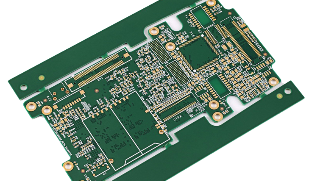
Blind and buried vias offer several advantages over standard through-hole vias:
- Higher routing density – By only connecting the required layers, blind/buried vias consume less space compared to a via that goes through the entire board. This enables more compact layouts.
- Signal isolation – Blind/buried vias prevent unwanted connections between layers that could cause signal integrity issues. The vias connect only the intended layers.
- Lower capacitance – Because they have less metal overlap between layers, blind/buried vias have lower parasitic capacitance than through-hole vias. This helps maintain signal integrity at high speeds.
- Flexibility – Blind/buried vias permit connections between non-adjacent layers, allowing flexible routing architecture not possible with through-hole vias.
- Improved manufacturability – Smaller holes are easier to plate and have improved hole wall quality. Buried vias are protected from smearing during lamination.
Design Considerations for Blind and Buried Vias
Here are some key factors to consider when working with blind and buried vias in your PCB layout:
Layer Stack Planning
- Plan the layer stack with blind/buried vias in mind. Group signals that need connections into adjacent layers.
- Minimize the number of layers spanned by blind vias for easier manufacturing.
- Ensure sufficient separation between buried vias and outer layers to meet voltage isolation requirements.
Via Size and Spacing
- Use smaller drill sizes like 0.2mm to 0.3mm to maximize routing density. Ensure your board shop can meet your minimum via size needs.
- Allow adequate spacing between vias for the required hole wall copper thickness. This is usually around 20% of the drill diameter.
Via Tenting
- Tenting refers to covering blind/buried via holes with soldermask. This prevents solder or debris from entering the vias during assembly.
- Larger vias may require plugging with epoxy or copper plating for tenting. Smaller vias can typically be tented with just soldermask.
Lane-to-Lane Spacing
- Use larger spacings between blind/buried via lanes routed in parallel to prevent solder wicking between lanes during assembly.
Testing and Inspection
- Verify electrical connectivity through 100% electrical testing. Optical inspection alone may not be sufficient.
- For buried vias, specialized test points or fixtures may be needed to probe inside the PCB stackup.
Implementation Guidelines
Follow these best practices when designing with blind and buried vias:
- Use blind vias to route between surface layers and immediately adjacent inner layers only. Minimize the number of layers spanned.
- Reserve buried vias for connections only between internal layers. Do not attempt to connect buried vias to surface layers.
- When routing differential pairs, keep the vias in each pair close together and match their layer spans. This maintains consistent coupling and timing.
- For high-speed signals, place ground vias adjacent to signal vias to provide a return path. Use ground planes between signal layers if possible.
- Remove unused vias and backfill them with epoxy to avoid creating tunnels for EMI or moisture ingress.
- In congested BGA fanout regions, consider dogbone routing (trace-via-trace) to access blind/buried vias. This expands the routing channels.
- To reduce congestion, divert less critical signals to different board areas when possible. Use blind/buried vias for high-priority signals only in constrained regions.
Summary
Blind and buried vias are key enablers for complex, high-density PCBs required in today’s electronics. By providing targeted layer connections without consuming through-hole real estate, blind and buried vias unlock routing architectures not possible with standard vias alone.
To leverage their full potential, you need to plan your layer stack and design rules carefully around these special vias. Follow the guidelines in this article, and you will be well on your way to employing blind/buried vias successfully in your next PCB design.
Frequently Asked Questions
Q: What is the difference between blind, buried, and through-hole vias?
A: Blind vias connect an outer layer to one or more inner layers, but do not go through the entire board. Buried vias connect two or more inner layers only. Through-hole vias span the entire board layers from top to bottom.
Q: When should blind/buried vias be used instead of through-hole vias?
A: Use blind/buried vias when you need connections between non-adjacent layers or when high routing density is required. The reduced drill size and lack of through-hole connection enables greater layout efficiency.
Q: What are some ways to maximize routing density with blind/buried vias?
A: Using smaller via sizes, careful layer planning, adequate via spacing, and techniques like dogbone routing all help optimize routing density when using blind/buried vias.
Q: Do blind/buried vias reduce signal quality compared to through-hole vias?
A: Generally no – blind/buried vias offer better signal integrity by containing connections between fewer layers with lower associated capacitance and cross-talk. Proper layer stack planning is important however.
Q: How can I test buried and blind vias on my PCB?
A: Testing can be done with specialized test points, fixtures, and 100% electrical testing. Additional optical inspection may also help but is not sufficient alone due to the inability to visually examine all layers.
Leave a Reply