Introduction to Bare PCBs
A printed circuit board (PCB) forms the backbone of any electronic device. It provides the mechanical structure to mount and interconnect electronic components using conductive copper traces etched from copper sheets laminated onto a non-conductive substrate.
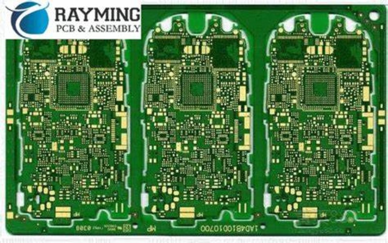
Bare PCBs contain only the bare minimum – a laminated board with etched copper traces and mounting holes. They contain no components and require additional assembly to solder components onto the board.
Bare PCBs allow creating customized PCB designs cost-effectively in low volumes. This makes them ideal for prototyping and low-volume production runs. Mass-produced PCBs are more cost-effective for large production volumes.
This article provides a detailed overview of bare PCB manufacturing, covering:
- PCB design and layout
- PCB fabrication process
- PCB assembly
- PCB testing and inspection
- Factors affecting PCB cost
- Choosing a PCB manufacturer
PCB Design and Layout
Schematics Capture
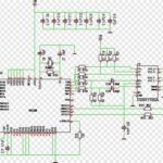
PCB design starts with capturing the circuit schematics. It defines the electronic components and their interconnections required for the circuit function. Common schematic capture software options are:
- Altium Designer
- Cadence Allegro
- Mentor Graphics Xpedition
- Zuken CR-8000
Schematics are crucial for PCB design as they enable simulation of the circuit to verify the PCB layout will function correctly.
PCB Layout
The PCB layout involves mapping the schematic onto a 2D layout with appropriate component footprints and routing copper traces between components.
Key considerations during PCB layout:
- Component placement – optimize for efficient routing and minimize trace lengths
- Routing – ensure traces are appropriately spaced for the target PCB fabrication process
- Impedance control – match trace impedance to schematic requirements
- High-speed signals – carefully route to minimize interference
- Stackup – ensure adequate layer count and dielectric materials
- Fabrication/assembly – ensure design is manufacturable
Common PCB layout software options are:
- Altium Designer
- Cadence Allegro
- Mentor Graphics Xpedition
- Zuken CR-8000
Design Rule Checking
Design rule checking (DRC) software scrutinizes the PCB layout to identify any violations of the target PCB fabrication process capabilities. Common checks include:
- Minimum trace width/spacing
- Minimum hole size
- Trace width changes
- Annular ring size
- Plane connection errors
Fixing DRC errors ensures the PCB can be fabricated correctly.
Generate Manufacturing Outputs
The PCB layout software generates the necessary outputs for PCB fabrication and assembly, including:
- Gerber files – vector image files defining copper layers, solder mask, silkscreen, etc.
- Drill files – NC drill file containing hole sizes and locations
- BOM – bill of materials listing all components
- Centroid file – coordinates for component placement
- 3D models – for checking assembly clearances
PCB Fabrication Process
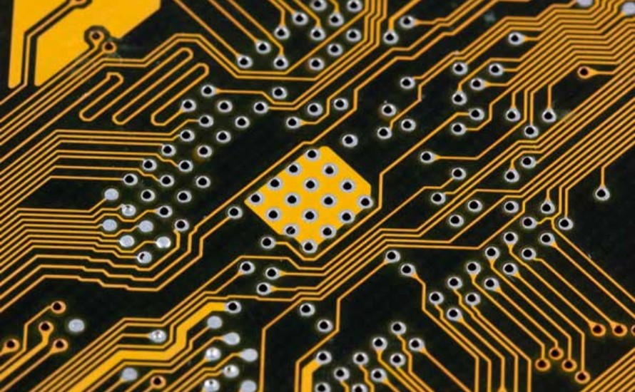
PCB fabrication involves complex processes to transform raw materials into finished boards. Understanding these processes helps optimize PCB design and choose the right PCB manufacturer.
Laminate Production
The PCB fabrication process starts with producing the laminate – the raw PCB substrate material. The laminate composition depends on the PCB’s performance requirements. Some common laminate types are:
- FR-4 – Glass-reinforced epoxy resin, suitable for most general-purpose PCBs
- Polyimide – Extremely heat resistant for flex PCB applications
- Rogers – PTFE-based laminates for high-frequency applications
- Ceramic-based – For high thermal performance
Laminate sheets consist of woven glass fabric bonded with resin cured under high temperature and pressure. The material, resin content, weave styles and thicknesses define the laminate’s properties.
Inner Layer Fabrication
PCBs typically consist of alternating layers of copper and core laminate. The inner layer fabrication process is:
- Drilling – The laminate sheet is drilled with small registration holes for alignment between layers.
- Hole metallization – The walls of drilled holes are made conductive by electroless copper plating.
- Photolithography – A photoresist dry film is laminated on the copper foil side of the core. The resist is then selectively exposed to UV through a photomask and developed. This transfers the PCB pattern onto the photoresist.
- Etching – The exposed copper is etched away, leaving only the desired copper pattern protected by photoresist.
- Stripping – The remaining photoresist is stripped away, revealing the finished inner layer.
The process is repeated to produce all required inner layers, which are precisely aligned using the registration holes.
Laminating Inner Layers
The etched inner layers are stacked in alignment and laminated together under high temperature and pressure. The laminate cores act as insulating dielectric layers between the copper layers.
Additional laminate sheets may be added as the outermost layers. The laminated PCB stack is a complete circuit ready for further processing.
Outer Layer Processing
The outer layers go through a similar photolithography process as the inner layers to define the outer copper layers:
- Drilling – Via holes are drilled through the entire laminate stack to interconnect inner and outer layers.
- Plating – Copper is plated onto the via holes to make them conductive.
- Patterning – The outer layers are coated with photoresist and patterned to produce the desired copper traces.
- Etching – Exposed copper is etched away, leaving only the photoresist-protected copper circuitry.
- Stripping – Photoresist is chemically stripped.
This completes the conductive copper patterning required for the PCB function.
Soldermask and Silkscreen
Additional non-conductive layers are added to protect copper traces and mark component locations:
- Soldermask – Epoxy-based layer covering exposed copper to prevent solder bridges. Openings left around pads.
- Silkscreen – Printed layer for component designators and polarity markings.
These layers complete the bare PCB fabrication. The boards now undergo final finishing.
Final Finishing
- Bevelling – Edges smoothed to remove sharp corners
- Routing – Individual boards cut from the fabrication panel
- Hole plugging – Unused holes plugged for structural rigidity
- Cleaning – Flux residues chemically cleaned
- Electrical testing – Each board tested for short circuits
This completes the PCB fabrication process. The finished boards are now ready for component assembly.
PCB Assembly Process
Assembling components onto the bare PCB converts it into a functional electronic circuit. There are two mainstream PCB assembly processes:
Through-Hole Assembly
Through-hole components have wire leads that pass through holes in the PCB and are soldered for both mechanical and electrical connection.
Typical through-hole assembly steps are:
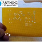
- Screen printing – Solder paste applied onto pads
- Component placement – Components inserted into board either manually or using pick-and-place
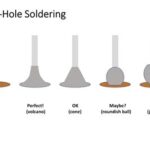
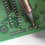
- Soldering – Board passed through wave soldering machine or reflow oven to melt solder paste and attach components
- Cleaning – Flux residues washed off
- Inspection – Visual or automated optical inspection (AOI)
- Testing – In-circuit testing validates board function
Through-hole assembly can be automated but requires relatively large pad sizes and hole diameters.
Surface-Mount Assembly
Surface-mount components have metallized contact pads that directly solder onto corresponding pads on the PCB surface. This enables smaller component sizes and lead pitches.
Typical SMT assembly steps are:
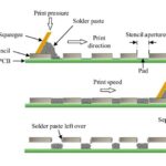
- Screen printing – Solder paste stenciled onto pads
- Pick-and-place – Robotic machine precisely places components onto pads
- Reflow soldering – Board passed through conveyor oven to melt solder paste and attach components
- Cleaning – Flux residues washed off
- Inspection – AOI checks placement accuracy and solder joints
- Testing – Validates board functionality
SMT assembly offers higher automation, density and throughput than through-hole assembly.
PCB Testing and Inspection

Testing and inspection of assembled PCBs verifies assembly quality and catches any defects before shipment:
- In-circuit test (ICT) – Applies test vectors and measures responses to validate circuit functionality. Catches assembly errors like missing/wrong components or bad solder joints.
- Flying probe testing – Uses movable probes to electrically testconnectivity between points. Checks for shorts, opens, resistance.
- Automated optical inspection (AOI) – Camera-based inspection of solder joints. Identifies problems like insufficient solder, shorts, tombstoning.
- X-ray inspection – Captures X-ray images through the PCB to detect issues like open vias, shorts, foreign objects, voids in solder joints.
- Boundary scan – Tests interconnects between components with embedded boundary scan circuitry.
- Mechanical testing – Applies mechanical stress like vibration, shock, torque to validate robustness.
- Environmental stress testing – Subjects boards to extreme temperatures, humidity, altitudes.
Thorough testing and inspection safeguards against potential field failures and avoids expensive rework costs.
Factors Affecting PCB Cost
The cost of manufacturing bare PCBs depends on various factors:
- Board size – Larger boards use more materials and cost more.
- Layer count – Additional layers increase lamination costs. High layer counts (>12) require HDI technology.
- Laminate material – Exotic materials cost more than standard FR4.
- Trace/space – Finer lines and spaces need more process steps.
- Hole size/pitch – More tightly spaced vias increase drilling time and cost.
- Soldermask type – LPI masks cost more than traditional liquid soldermask.
- Finished copper – Immersion gold costs more than basic HASL finish.
- Special requirements – Impedance control, controlled dielectrics, buried/blind vias all add cost.
- Lead time – Rush orders often command premium prices.
- Order volume – High volumes benefit from economies of scale.
- Testing/inspection – Extensive testing and inspection increases cost.
- Location – Manufacturing cost varies among geographic regions.
Choosing A PCB Manufacturer
Here are some key considerations when selecting a PCB manufacturing partner:
- Capabilities – Ensure their processes and certifications match your requirements.
- Quality – Review previous customer testimonials and qualification reports. Tour their facilities.
- Technical support – Evaluate their design review and DFM analysis services.
- Prototyping – Choose a shop with quick-turn prototype abilities.
- Supply chain – Ensure access to raw materials and component sourcing.
- Testing capabilities – Availability of advanced test and inspection equipment.
- Facilities – Modern manufacturing environment with quality standards certification.
- Pricing & MOQs – Balance cost savings versus minimum order quantities.
- Logistics – Ability to consistently handle shipping, customs, local support.
- Ecosystem – End-to-end production including assembly and post-PCB services.
Taking the time to find the right PCB partner ensures you get high-quality boards delivered reliably at the best value.
Frequently Asked Questions
What are some key differences when designing a 4-layer vs 6-layer PCB?
Some considerations for 4-layer vs 6-layer PCB designs:
- Routing complexity – 6 layers offer more routing flexibility for complex, high-density designs. 4 layers can be limiting for intricate routing.
- Signal layers – 6 layers provide 4 signal layers versus just 2 with 4-layer boards. More signal layers reduce the need for compromises in trace routing.
- Impedance control – 6 layers enable a symmetrical stackup which gives better impedance control for high-speed signals.
- EMI control – The extra ground layers in 6 layers help isolate noise and provide better EMI control.
- Manufacturing cost – 6-layer PCBs require additional lamination cycles and cost more to fabricate.
- Flexibility for future revisions – 6 layers provide more margin for adding functionality in future board spins.
In summary, 6 layers are preferable for complex, high-speed or high-density designs despite the higher fabrication cost. Simpler designs can readily use 4 layers.
What are the tradeoffs between 0.5mm vs 1.0mm PCB thickness?
Key considerations for 0.5mm vs 1.0mm PCB thickness:
- Stiffness – Thinner 0.5mm boards can bend more easily. 1.0mm boards provide more mechanical rigidity.
- Weight – 0.5mm boards weigh about half as much as 1.0mm boards. Good for lightweight designs.
- Component height – Low profile components are required on 0.5mm boards. Tall components may require 1.0mm or thicker.
- Routing space – Thinner 0.5mm boards provide less vertical routing space between layers.
- Layer count – 0.5mm boards are typically limited to 2-4 layers. High layer counts require 1.0mm or more.
- Warping – Thinner boards are more prone to warping during fabrication and assembly.
- Cost – 0.5mm boards use less materials so can cost marginally less.
- Flexibility – 0.5mm boards are better suited for simple rigid-flex designs.
In summary, 0.5mm boards are well suited for small, portable and low-cost designs. 1.0mm boards are preferable for more complex, multilayer PCBs requiring mechanical rigidity.
How are impedance controlled traces implemented on PCBs?
Some common techniques for implementing impedance controlled traces on PCBs:
- Matching trace width – Using precise matched trace widths, typically paired differential traces.
- Reference planes – Solid uninterrupted ground/power planes adjacent to trace for controlled impedance.
- Dielectric selection – Choosing PCB substrate dielectric to achieve target impedance.
- Symmetric stackup – Using identical dielectric layers above and below trace.
- Trace spacing – Carefully spacing traces from planes or each other to control impedance.
- Thin dielectrics – Using very thin high-performance dielectrics.
- Buried/embedded traces – Controlling impedance by embedding trace between power/ground layers.
- No coverlayer – Eliminating soldermask over traces prevents dielectric variations.
- Trace thickness/width ratio – Varying trace thickness and width proportionally to achieve impedance.
Simulation and controlled processes during fabrication are necessary to successfully implement impedance controlled routing.
What are the main advantages of using a soldermask layer on the PCB?
Some key advantages provided by the soldermask layer on a PCB include:
- Preventing solder bridges – Soldermask prevents solder from bridging between closely spaced pads during assembly.
- Protecting traces – It coats exposed traces to prevent oxidation and prevent tracing shorts.
- Insulation – Soldermask provides additional insulation and isolation between traces.
- Marking solder areas – Openings in soldermask cleanly define solderable areas on pads.
- Component marking – Acts as the background for component designators and polarity markings.
- Aesthetics – Provides a neat, clean appearance compared to bare copper traces.
- ESD/EMI protection – Can help control electrostatic discharge and electromagnetic interference when used as a surface finish.
- Moisture resistance – Masks help protect board from environmental exposure and moisture ingress.
So in summary, soldermasks are indispensable for reliable PCB protection, insulation and aesthetics.
What are some key inspection criteria when evaluating a fully assembled PCB?
Some key aspects to inspect on an assembled PCB are:
- Component placement – Verify all components are present and placed in the right locations/orientations.
- Solder joints – Inspect that solder joints are fully formed and have acceptable fillet shapes. Look for problems like insufficient solder, cracks, bridging.
- Solder balls/splatter – Check for any loose solder residues shorting pads.
- Crimps/markings – Ensure component leads are not damaged from insertion.
- Residual flux – Look for any remaining flux residues left after cleaning.
- Warping/twisting – Board should be flat without warps or twists.
- Mechanical defects – Inspect for any cracks, scratches, handling damage on the board.
- Annular rings – Confirm annular rings around plated through-holes meet minimum requirements.
- Electrical testing – Perform in-circuit testing, boundary scan, functional testing to validate board operates correctly.
Paying close attention to these areas helps catch assembly defects early and ensures only quality boards ship out.
Leave a Reply