Introduction to Automated Circuit Board Assembly
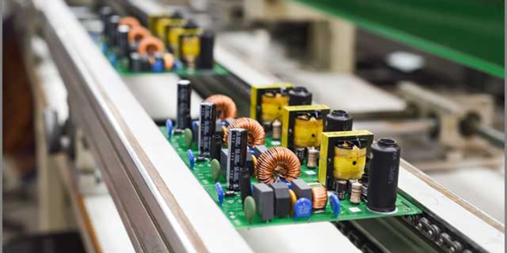
Printed circuit boards (PCBs) are essential components in nearly all modern electronics. They provide the foundation on which microchips, resistors, capacitors and other components are mounted and connected to create functional electronic devices. The assembly of PCBs has traditionally been a manual process requiring skilled technicians, but in recent years automated circuit board assembly has become increasingly common.
Automated assembly offers numerous advantages over manual methods, allowing PCB manufacturing and electronics companies to improve quality, increase throughput and reduce costs. This article will provide an overview of automated circuit board assembly, examining the key technologies involved and their benefits. It will also look at the future outlook for automation in PCB production.
Overview of the PCB Assembly Process
PCB assembly consists of soldering electronic components onto the boards according to the design schematics. This involves a number of steps:
- PCB Printing – The circuit board blanks are made from laminated sheets of copper and fiberglass substrate material. Using photolithography techniques, the desired circuit pattern is printed onto the boards.
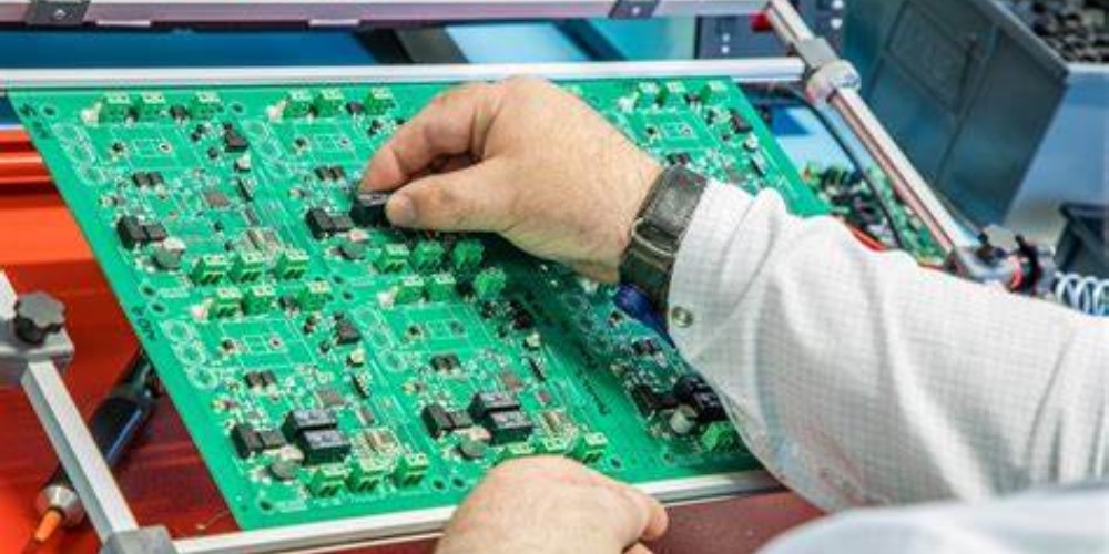
- Component Placement – Electronic components are precisely positioned onto the PCBs. This may be done manually or by automated pick-and-place machines.
- Soldering – The components are soldered to the boards to create electrical connections and permanently attach them. Wave soldering and reflow ovens may be used.
- Inspection and Testing – Assembled boards are visually inspected and then tested electronically to verify functionality.
- Conformal Coating – A protective coating may be applied to prevent damage from moisture and contaminants.
Automated assembly introduces automation into many of these processes, especially component placement and soldering.
Benefits of Automated Assembly
Automating PCB assembly provides electronics manufacturers with a wide array of benefits:
Higher Productivity and Throughput
- Automated pick-and-place machines can place tens of thousands of components per hour, far exceeding manual assembly.
- Parallel processing with multiple assembly lines increases total output.
- Automated optical inspection is faster than manual methods.
This increased efficiency enables companies to meet higher production demands cost-effectively.
Improved Quality and Consistency
- Automated processes perform repetitive tasks consistently without fatigue or human error.
- Automated soldering provides even heating and minimizes defects like cold joints.
- Automated inspection accurately identifies flaws down to microscopic size.
This boosts yields, reduces rework and field failure rates.
Lower Labor Costs
- Reduced need for skilled technicians and operators to perform assembly.
- Automation enables 24/7 unmanned production.
This provides significant cost savings, especially relevant with rising labor costs worldwide.
Flexibility and Scalability
- Automated assembly lines can be reprogrammed for different PCBs.
- Production capacity can be rapidly scaled.
This allows companies to respond to changing production needs and new product introductions with minimal disruption.
Key Technologies for Automated PCB Assembly
Several technologies are central to enabling automated circuit board assembly:
Solder Paste Printing
Solder paste is first applied to PCBs to temporarily hold components in place before soldering. Automated print-and-dispense machines precisely deposit tiny amounts of solder paste onto pads using stencils or needle dispensers. This ensures accurate and consistent application.
| Method | Description |
|---|---|
| Stencil Printing | A metal stencil is temporarily fixed onto the PCB and solder paste is applied across it. |
| Needle Dispensing | Precisely positioned needles deposit tiny solder dots onto individual pads. |
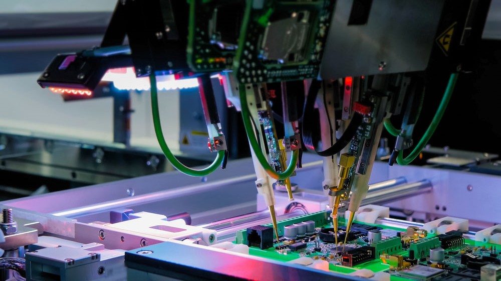
Pick-and-Place Machines
Pick-and-place machines use vacuum nozzles to pick surface-mount components from reels and accurately place them onto PCBs. Sophisticated computer vision aligns components and advanced nozzle designs reliably handle even ultra-small microchips. Flexible feeder setups allow loading of different component types.
| Metric | Capability |
|---|---|
| Speed | Up to 150,000 chips per hour |
| Placement Accuracy | As low as 0.025mm |
| Component Size | As small as 0201 chips (0.6mm) |
Reflow Soldering
Heating pre-applied solder paste melts it to produce permanent solder joints holding components in place. Reflow ovens use precisely controlled heating profiles to uniformly heat the assembly without damaging sensitive components. The process is fully automated for consistent results.
Conformal Coating
Protective plastic coatings applied using automated spray or selective dispensing equipment shield assembled PCBs from moisture, dust and chemicals. Coatings safeguard against corroded joints and short circuits during product use.
Automated Inspection
Machine vision systems rapidly scan assembled PCBs to identify defects like missing or misaligned components. Powerful image processing software can detect flaws down to 0.5mm. This prevents further processing of defective boards.
The Future of Electronics Assembly Automation
Automation has already been widely adopted, but continuing innovation is expanding its applications:
- Miniaturization – Improved nozzle and feeding systems allow automated placement of tiny 01005 and 0201 components.
- Advanced Robotics – Robotic arms offer greater speed, precision and flexibility for pick-and-place and inspection applications.
- AI and Machine Learning – Vision systems are incorporating AI for smarter defect detection and quality control.
- Additive Manufacturing – 3D printing of PCBs and embedded component integration will reduce assembly steps.
These developments will enable automation to tackle more complex assembly tasks, driving electronics production efficiencies even higher. As global demand for electronics continues rising, automated assembly will be critical for future industry growth and competitiveness.
Frequently Asked Questions
What are the main benefits of automated PCB assembly?
The primary benefits are increased throughput, improved quality consistency, lower labor costs and greater manufacturing flexibility compared to manual assembly. This allows companies to meet rising production needs cost-effectively.
What are some key enabling technologies for automation?
Critical technologies include solder paste printers, automated pick-and-place machines, reflow ovens, conformal coating systems and automated optical inspection. Continued improvements are expanding automation capabilities.
How widely adopted is assembly automation currently?
Automation is already widely used, especially by large-volume electronics manufacturers. Over 75% of PCB assemblies for consumer devices are estimated to be produced using automated processes.
Does automation eliminate PCB assembly jobs?
While reducing direct labor requirements, automation creates new jobs in equipment maintenance, process engineering and quality control. Overall employment impact depends on a company’s growth and production expansion.
What is the future outlook for assembly automation?
Ongoing advances in robotics, machine learning and additive manufacturing will drive further automation. This will enable increased miniaturization, flexibility and integration for electronics manufacturing.


Leave a Reply