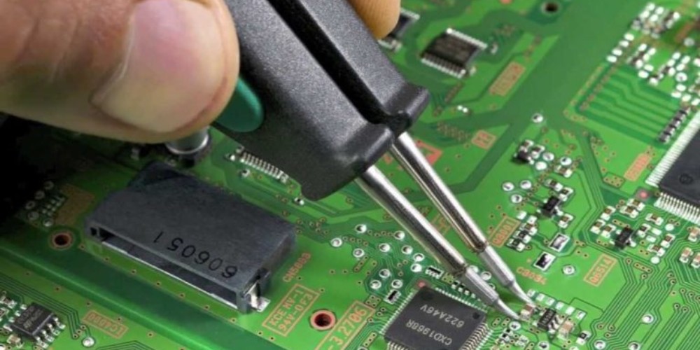
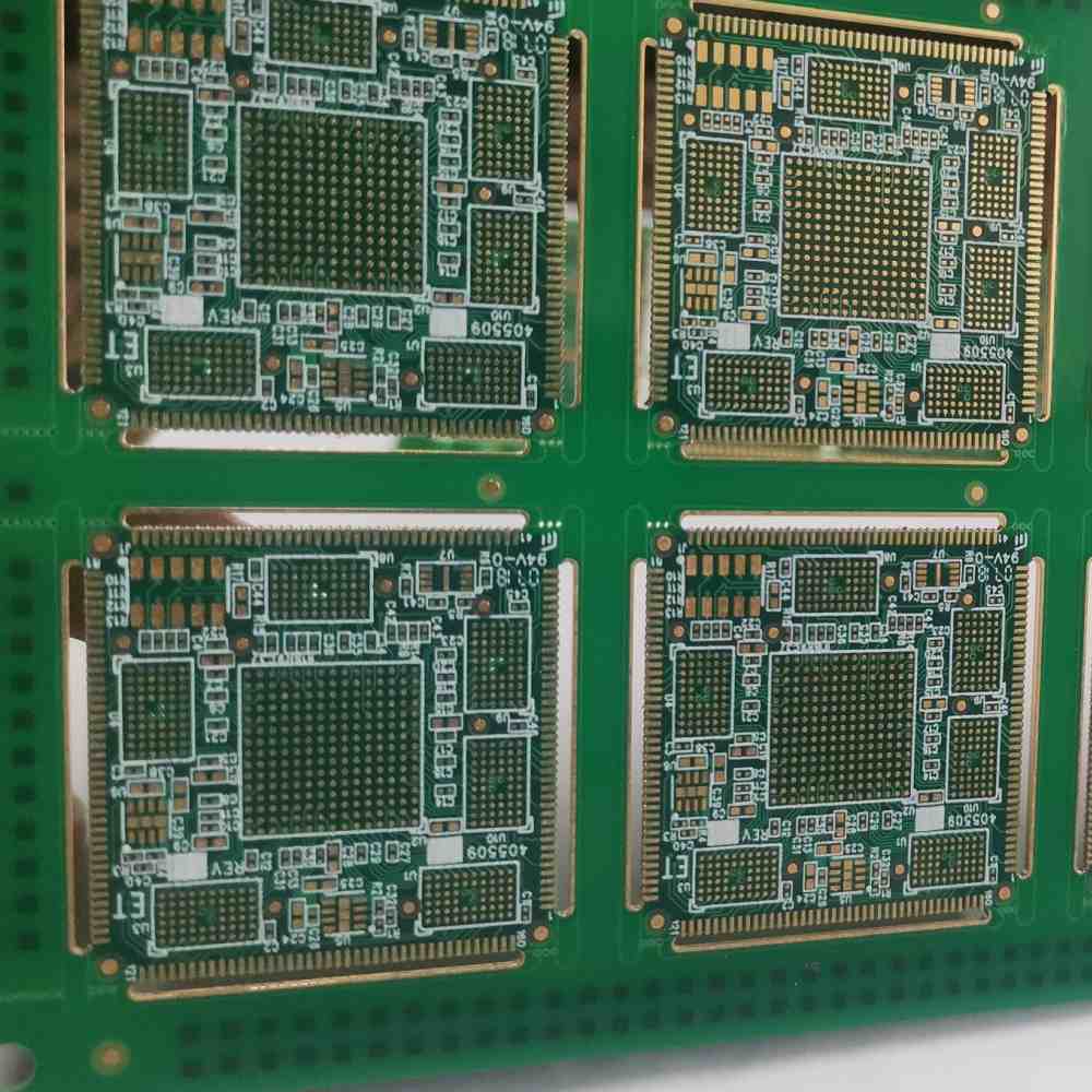
Buried vias are an important component in printed circuit boards (PCBs) that allow connections between different layers in the board. A key question that arises is whether these vias are filled or unfilled. The answer has implications for manufacturability, reliability, and performance of the PCB. This article provides an in-depth look at buried vias, whether they are filled, the filling process, and the pros and cons of filled vs unfilled vias.
What are Buried Vias?
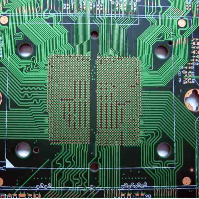
Buried vias are vias that connect inner layers of a multi-layer PCB while being completely enclosed within the PCB stackup. They allow interconnections between layers that are neither the top nor bottom layers.
For example, consider a 6-layer board with layers ordered as:
- Top Layer
- GND Plane
- Power Plane
- Signal Routing Layer 1
- Signal Routing Layer 2
- Bottom Layer
Vias between Layers 1 and 6 are considered through-hole vias. However, vias between inner layers like Layers 2-3, 2-4, 3-4 are considered buried vias since they do not connect to an outer layer.
Key properties of buried vias:
- Connects two or more inner layer pads
- Does not connect to top or bottom layer pad
- Fully enclosed within PCB stackup
- Difficult to probe or repair if defective
- Smaller diameter than through-hole vias
- Formed by laser drilling during PCB fabrication
Are Buried Vias Filled?
The majority of buried vias in modern PCBs are filled vias. That means the via barrel is filled with a conductive material like copper after drilling to form a solid connection between the two inner layers.
There are a few main ways that buried vias can be filled:
- Plated fill – The most common method. The via is plated with copper electrolessly first. Then pattern plating adds copper thickness. The plating connects the walls of the via barrel between the two pads.
- Plugged/tented vias – A copper rivet or plug is inserted into the via manually after drilling. The rivet connects the via pads.
- Conductive ink fill – The via barrel is screen printed with conductive ink, such as polymer thick film silver. The ink is then cured to form the interconnect.
- Conductive epoxy fill – A conductive epoxy can be dispensed into the via to form the interconnect after curing.
Here is a table comparing different via filling methods:
| Method | Process Overview | Cost | Reliability |
|---|---|---|---|
| Plated fill | Plate copper on via barrel walls | Low | High |
| Plugged via | Insert conductive rivet in via | Medium | Medium |
| Ink fill | Screen print then cure conductive ink | Medium | Low-Medium |
| Epoxy fill | Dispense then cure conductive epoxy | High | Medium |
As the table shows, plated filling is the most common and reliable process due to its low cost. Ink or epoxy filling may be used for specialized applications.
Why Fill Buried Vias?
Filling buried vias provides several benefits compared to leaving them hollow including:
- Increased current capacity – The copper fill offers much higher conductance than an air-filled hole. This allows more current to flow through the via.
- Improved structural integrity – Filling adds mechanical strength. Unfilled vias can crack or cause separation in the Z-axis.
- Reduced emanation – A void can act as a slot antenna, emitting EMI. Filling prevents leakage of signals between layers.
- Easier soldering – The flat top surface reduces solder wicking down into the via during soldering of components.
- Better plating distribution – Plating becomes more uniform between pads with a filled via.
- Improved heat dissipation – Filled vias conduct heat better between layers.
There are some downsides to filled vias to consider as well:
- Increased cost and fabrication time – The filling process adds steps to PCB production.
- Potential for voids – Improper filling can leave hidden voids.
- Disturbed signal return paths – May need back-drilling for RF/high-speed signals.
Buried Via Filling Process
Here is an overview of the typical buried via filling process using plated copper:
- Drill vias – A laser drills blind vias connecting the required inner layer pads. The vias initially are hollow through holes.
- Seed layer deposition – A thin seed layer of copper is sputtered onto the walls of the drilled holes.
- Electroless copper plating – An electroless bath deposits a thin layer of copper (0.5-1μm) atop the seed layer. This coats the entire via barrel with conductive copper.
- Photoresist application – Photoresist is applied and imaged to mask off areas that won’t receive further plated copper. The vias remain unmasked.
- Pattern copper plating – Electroplating in an acid copper bath deposits a thicker copper layer (10-20μm) within the vias to fill them.
- Photoresist stripping – The photoresist is chemically stripped away, leaving the filled vias.
The plated copper completely fills the via to create a solid conductive connection between the layers. Additional processes refine the shape of the via.
Here is an illustrated overview of this typical buried via filling process using plated copper:
| Step | Illustration |
|---|---|
| 1. Drilling | Show Image |
| 2. Seed Layer | Show Image |
| 3. Electroless Plating | Show Image |
| 4. Photoresist Application | Show Image |
| 5. Pattern Plating | Show Image |
| 6. Photoresist Stripping | Show Image |
This plating process produces a filled via with a conductive copper interconnect between layers. The via is structurally reinforced and has low electrical resistance.
Unfilled Buried Vias
While most buried vias are filled, there are some cases where unfilled or partially filled vias may be used.
Reasons to use unfilled buried vias include:
- Cost reduction – Eliminates filling steps for non-critical vias.
- Thermal isolation – Air provides insulation between layers.
- Backdrilling – Allow easy via stub removal.
- Impedance control – The air void lowers capacitance for high-frequency signals.
- Venting – Permits outgassing and pressure equalization.
Partially filled vias can also be specified, where only a thin seed layer coats the barrel. This offers a compromise between electrical conduction and thermal isolation.
However, leaving vias completely unfilled risks cracking or separation failure. It also increases EMI compared to filled vias. Careful structural analysis is required to ensure reliability.
Here are some applications where unfilled buried vias may be suitable:
- Non-critical stitching vias.
- RF circuits where lowering capacitance is critical.
- High power boards requiring thermal isolation between layers.
- Quick-turn low cost prototype PCBs.
So in summary, while most production boards have filled buried vias, unfilled vias can be advantageous in certain specialized applications provided mechanical integrity is thoroughly analyzed.
Should You Fill Your Buried Vias?
For most standard PCB applications, filling buried vias is recommended. The benefits of increased robustness and current capacity outweigh the small increase in fabrication time and cost.
Here are some guidelines on when to fill buried vias in your design:
- Fill all vias carrying significant current flow. The reduced resistance is critical.
- Fill vias in high vibration/shock environments. Filling prevents cracking.
- Fill vias with sensitive signals like clock or data lines. This reduces EMI.
- Fill vias transmitting high frequency signals. This prevents impedance discontinuities.
- Partially fill thermal vias between ground planes and power planes to balance electrical and thermal performance.
Exceptions where leaving vias unfilled may be acceptable:
- Vias connecting two different ground planes. The connections are non-critical.
- Redundant or non-critical vias for minor traces. Electrical performance is less important.
- Boards not subject to vibration/shock loads. Cracking is less likely.
- Short prototype runs where cost is most important. Performance is less critical.
So in summary, filled buried vias should be the default choice for most PCBs. Unfilled vias require careful analysis to ensure the cost or performance benefit outweighs the reduction in reliability and current capacity. Discuss via filling considerations with your PCB manufacturer early in the design process.
FAQ
What is the most common way buried vias are filled?
The most common method of filling buried vias is with plated copper. The via hole is first plated with a thin seed layer, then pattern plated with 10-20 μm of copper to fill the barrel completely.
What materials can be used to fill buried vias?
Common filling materials include copper, silver, conductive ink or epoxy, and solder. Copper offers the best conductivity and is most commonly used. Others are occasionally used for specialized applications.
What are the disadvantages of unfilled buried vias?
Unfilled buried vias have lower current capacity, reduced reliability, potential for EMI leakage, and poorer heat conduction between layers. The void also inhibits solder flow. Careful analysis is required if using unfilled vias.
How are partially filled vias created?
Partially filled vias are made by plating only a thin seed layer of copper on the via walls. This acts as a conductive coating but maintains an air gap in the barrel. It represents a compromise between electrical and thermal performance.
Can buried vias be repaired if defective?
Buried vias cannot be directly probed or repaired like through-hole vias. Filled buried vias in particular are difficult to repair. Ensuring quality fabrication the first time is critical for buried vias.


Leave a Reply