Introduction
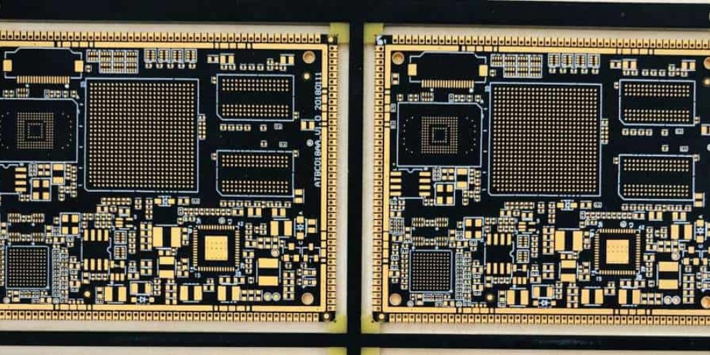
A via is a small hole that is drilled in a printed circuit board (PCB) and plated with a metal coating to electrically connect different layers together. Vias come in two main types – through-hole vias that span all layers of the PCB from top to bottom, and blind/buried vias that only connect two or more inner layers without reaching the outer surfaces.
Blind vias are vias that connect the inner layers of a multilayer PCB but do not go all the way through from the top to the bottom. They are “blind” from at least one outer surface. In contrast, through-hole vias span the entire PCB.
This article examines whether blind vias are indeed more expensive to implement than standard through-hole vias, and the reasons behind any cost differences.
Manufacturing Differences Between Blind and Through-Hole Vias
There are a few key differences in how blind vias and through-hole vias are manufactured, which contribute to cost variances:
1. Additional Drilling Steps
To create a blind via, the PCB manufacturer has to drill down to the required inner layers selectively. This requires using smaller stubbed drill bits only long enough to reach the inner layers and extra steps to change the drill bits between layers.
In comparison, a standard through-hole via can be drilled in one pass from top to bottom with a regular long drill bit. The additional drilling steps make blind vias take longer to manufacture.
2. More Complex Plating Process
The plating process is also more complex for blind vias. When plating through-hole vias, the plating metal can be flowed easily from one end straight to the other.
But for blind vias, the plating has to be done separately for the different segments of the hole. This also requires more precision and time.
3. Require Advanced Equipment
Blind and buried vias can only be manufactured on more advanced PCB fabrication equipment that can handle multi-layer boards and selective drilling and plating. Standard double-sided boards do not require these capabilities.
The more complex equipment involved contributes to higher fixed costs for facilities that can produce blind/buried vias.
Factors That Increase Blind Via Costs
Based on the manufacturing differences, here are some specific factors that can make blind vias costlier than through-hole vias:
Number of Layers
The more layers in a multilayer PCB, the more complex the blind via fabrication process becomes. For instance, a 6-layer board with blind vias between layers 2-5 would require more steps than a 4-layer board.
As the layer count increases, equipment requirements also become more stringent to enable drilling and plating different via depths accurately.
Aspect Ratio
The aspect ratio refers to the relationship between the diameter of the via and its depth. A higher aspect ratio means a deeper and narrower via.
Blind vias often need to be high aspect ratio to connect inner layers without consuming too much surface area. But deeper and narrower holes are harder to manufacture consistently.
Tolerance and Precision
Blind vias call for very tight tolerance and precision when drilling and plating. Even minute deviations can result in open or unreliable interconnects.
The high-precision needs results in lower manufacturing yields and higher costs.
Quantity
Setting up the equipment for blind/buried vias involves some fixed overhead time and costs. If the order volume is low, this can increase the costs per board. Larger orders help amortize the setup costs.
Location
If the blind vias are concentrated in one area rather than distributed evenly around the board, it requires more frequent drill bit changes. This slows down the process.
Size
Smaller blind vias are harder to manufacture than larger ones, due to the precision needed. And if different locations need different sized blind vias, it further complicates fabrication.
Cost Comparison Between Blind Vias and Through-Hole Vias
To illustrate the cost differences quantitatively, here is a comparison table with estimated costs in USD for sample 2-layer, 4-layer, and 6-layer PCBs with just standard through-hole vias versus using blind/buried vias:
| PCB Type | Layers | Via Type | Cost Per Board |
|---|---|---|---|
| 2-layer board | 2 | Through-hole vias | $50 |
| 4-layer board | 4 | Through-hole vias | $100 |
| 4-layer board | 4 | Blind/Buried vias | $250 |
| 6-layer board | 6 | Through-hole vias | $150 |
| 6-layer board | 6 | Blind/Buried vias | $350 |
The table shows how the use of blind/buried vias in multilayer boards can increase per-board fabrication costs significantly compared to just using through-hole vias. The more layers, the higher the cost differential.
Some key observations:
- Even for 2-layer boards, blind vias will be more expensive than through-hole but usually not prohibitively so. The big cost jump happens going from 2 to 4+ layers.
- The incremental cost of adding more layers is also higher for blind vias vs. through-hole vias.
- Blind vias on 4-layer boards can be 2-3x more expensive than all through-hole vias. On 6-layers, the blind via price is 2-4x higher.
- In absolute terms, blind vias on 6+ layer boards often cost $200+ per board higher than all through-hole vias.
So in summary, while blind vias enable greater routing flexibility on multilayer boards, they come at a significant premium over standard vias. The PCB designer has to decide whether the benefits justify the extra fabrication costs.
Reasons For Using Blind Vias Despite Higher Costs
Even with the higher expense, blind and buried vias are very commonly used on complex, high-density PCBs. Here are some key reasons that justify the extra costs:
1. Allow High-Density Interconnects on Multilayer Boards
Blind and buried vias permit connections between inner layers that minimize surface usage. This enables greater component density and trace routing flexibility.
Through-hole vias would block valuable surface real estate and limit layout options.
2. Reduce Layer Counts for Equivalent Routing
Blind/buried vias let PCBs achieve a similar level of interconnects with fewer layers compared to only using through-hole vias.
Although blind vias have a higher cost per layer, reducing layers lowers overall fabrication costs.
3. Improve Signal Integrity
Blind/buried vias allow signals to remain on inner layers for longer paths. This shields them from interference and noise, providing better signal integrity compared to bringing them up to the surface frequently.
4. Provide More Security
Keeping circuits contained within inner layers of a multilayer PCB makes it harder to probe and reverse-engineer a board. Blind and buried vias thus help improve security against copying and hacking.
5. Enable High-Density Fan-Out Routing
Technologies like fan-out wafer-level packaging with redistribution layers depend heavily on blind/buried vias to enable dense component interconnects.
6. Facilitate Board-Level EMI Shielding
Using blind/buried vias to connect grounded layers forms Faraday cages that help contain and block EMI emissions.
7. Allow Smoother Current Flows
Proper use of blind/buried vias enables different voltage domains and ground paths to stay on specific inner layers for maximum efficiency.
8. Improve Manufacturability and Yields
Strategically-placed blind vias can reduce the need for manual vias, which lowers assembly costs. And minimizing surface vias improves first-pass soldering yields.
Newer Technologies to Reduce Blind Via Costs
The PCB industry continues to develop newer manufacturing techniques to try to reduce the costs of producing blind and buried vias:
- Laser direct imaging can drill blind vias faster and with greater accuracy than traditional mechanical drilling.
- Plasma processes enable more effective desmear and metallization of blind via holes.
- Better registration techniques allow blind vias to be positioned more reliably across layers.
- Improved drilling equipment with faster bit changing reduces transition time between drilling steps.
- More advanced routing software helps optimize blind via placement during layout.
- Automated optical inspection makes it easier to detect blind via defects, improving yields.
- Moving to panel-scale manufacturing on larger boards increases scale and throughput.
Adoption of such newer technologies can potentially help lower blind via expenses in the future while retaining their advantages. But for now, the cost difference remains quite substantial compared to standard vias.
Conclusion
In summary:
- Blind vias entail more complex manufacturing steps including specialized drilling and plating processes. This makes them costlier to fabricate than traditional through-hole vias.
- The cost premium increases substantially with higher layer counts, tighter tolerances, smaller sizes, and greater densities.
- On multi-layer boards, blind vias typically cost 2-4x more than using only through-hole vias.
- The benefits of blind vias like routing flexibility and layer count reduction often outweigh the higher expenses for complex, dense PCBs. But designers need to strategically evaluate their usage.
- Ongoing improvements in manufacturing techniques and equipment may gradually reduce blind via costs over time but significant differences remain versus through-hole vias.
Frequently Asked Questions
Q: Are buried vias cheaper than blind vias?
A: No, buried vias are generally similar in cost or sometimes even more expensive than blind vias. This is because buried vias require more complex 2-step drilling and plating processes to connect inner layers without reaching either outer surface. Blind vias at least have one end accessible.
Q: Can blind via costs be reduced by using cheaper PCB materials like FR-4?
A: Not really. The base materials have minimal impact on blind via costs. The bulk of the price premium versus through-hole vias comes from the specialized drilling, plating, inspection, and handling required during fabrication. This holds irrespective of whether the board itself uses FR-4 or more exotic substrates.
Q: Does it make sense to use microvias on the surface and keep blind vias only for inner layers?
A: This can be a good compromise. Microvias on the outer layers consume much less space than through-hole vias. Combining them with selective blind vias provides most of the interconnect benefits at a lower cost than using blind vias throughout. So it’s an approach worth considering.
Q: Are the yield rates much lower on boards with blind vias?
A: If the blind vias are not properly designed and fabricated, yields can suffer due to reliability issues like opens or inadequate plating. But with strict process controls, the yield difference versus through-hole vias can be minimized. Proper via placement optimization is critical as well.
Q: Can blind/buried vias be avoided completely by using a PCB with more layers?
A: In theory, yes more layers could remove the need for blind/buried vias. But beyond a point, adding more layers with only through-hole vias becomes prohibitively expensive in itself. Using some optimized blind vias provides the best trade-off in most cases.


Leave a Reply