Introduction
Printed circuit boards (PCBs) are essential components in almost all modern electronics. As electronic devices become more complex and compact, there is an increasing need for PCBs that can accommodate more intricate circuit designs. This is where anylayer PCBs come in.
Anylayer PCBs allow traces and routing on any layer of the board, providing more flexibility compared to traditional 2-layer or 4-layer designs. In this article, we will examine the benefits of anylayer PCBs and why they are becoming the preferred choice for many electronics manufacturers.
What are Anylayer PCBs?
Traditional PCBs have a limited number of layers, usually 2 to 8. Routing tracks and traces are confined to the outer layers or a few inner layers. Anylayer PCBs break this constraint by allowing routing on any layer, including the entire thickness of the board.
With anylayer technology, circuits can be routed vertically across all layers. This provides far more routing channels compared to standard multilayer boards. Components and vias can also be placed on any layer. Anylayer PCBs offer the ultimate in flexible and dense routing for complex, space-constrained designs.
Key Characteristics of Anylayer PCBs
- Routing and traces on any layer from top to bottom
- Components and vias can be placed on any layer
- Allows vertical interconnections through the entire board thickness
- Significantly higher routing density compared to standard multilayer PCBs
- Complex routing paths can be completed with fewer layers
Benefits of Using Anylayer PCBs

Anylayer technology offers several advantages over conventional multilayer boards:
Higher Routing Density
With routing channels available across all layers, anylayer PCBs can pack in a lot more circuitry in a given footprint. Components take up space on the outer layers, limiting routing on standard designs. Anylayer technology moves components inside while utilizing the entire thickness for traces. This enables far denser routing for complex and compact electronics.
Design Flexibility
Anylayer PCBs provide the ultimate routing flexibility. With no constraints on which layers can host traces, designers have complete freedom to route tracks vertically and horizontally. This allows efficient routing of high-speed, RF, and other critical signals. Dense board sections can be relieved by moving routing paths inside the board.
Lower Layer Count
The increased routing density means that anylayer PCBs can achieve layouts that would typically require 12-16 layers on a standard multilayer board. The high layer counts increase costs and fabrication complexity. With anylayer technology, equivalent routing can be completed with fewer layers, reducing costs.
Better Performance
Placing components inside the board and closer to inner layers allows for shortening of critical nets. This improves signal speed, integrity and overall circuit performance. The flexible routing also allows impedance control and matching for signals like PCIe or memory buses. Many anylayer PCBs require no micro-vias for interlayer connections. This avoids via-induced issues like reflections or ringings.
Miniaturization
Anylayer technology is ideal for complex and compact product designs. Routing tracks vertically provides high density in a small footprint. This allows reducing the overall PCB size while retaining complexity and component counts. Miniaturization is especially useful for handheld or portable electronics.
Lower Costs
Although anylayer PCBs use advanced processes, they can actually reduce costs compared to equivalent high layer count boards. A 16 layer anylayer may replace a 24 layer standard PCB with better characteristics. Lower layer PCBs cost less to fabricate. They also have higher yields and lower scrap/rework rates. This makes anylayer technology cost-effective for complex designs.
Applications of Anylayer PCBs
Anylayer PCBs are suitable for products where size, complexity, and performance are critical factors. Here are some typical applications:
- Consumer Electronics – Smartphones, tablets, IoT devices. The compact form factors and tight integration require high density PCBs.
- Automotive Electronics – Engine control units, infotainment systems, ADAS. Miniaturization and signal integrity are necessities.
- Aerospace/Defense – Avionics, navigation, and weapon systems. Ruggedness and reliability are needed along with density.
- Medical Electronics – Implants, imaging systems. Smaller and reliable boards are important.
- High Speed Computing – Servers, network/telecom gear. High speed interfaces and signal quality matter.
Anylayer PCBs are also used for RF designs like 5G antennas and radars. The vertical routing helps controlling impedance across layers.
Overall, anylayer PCB technology provides the most benefit where reliability, high density, and electrical performance are key metrics along with small size.
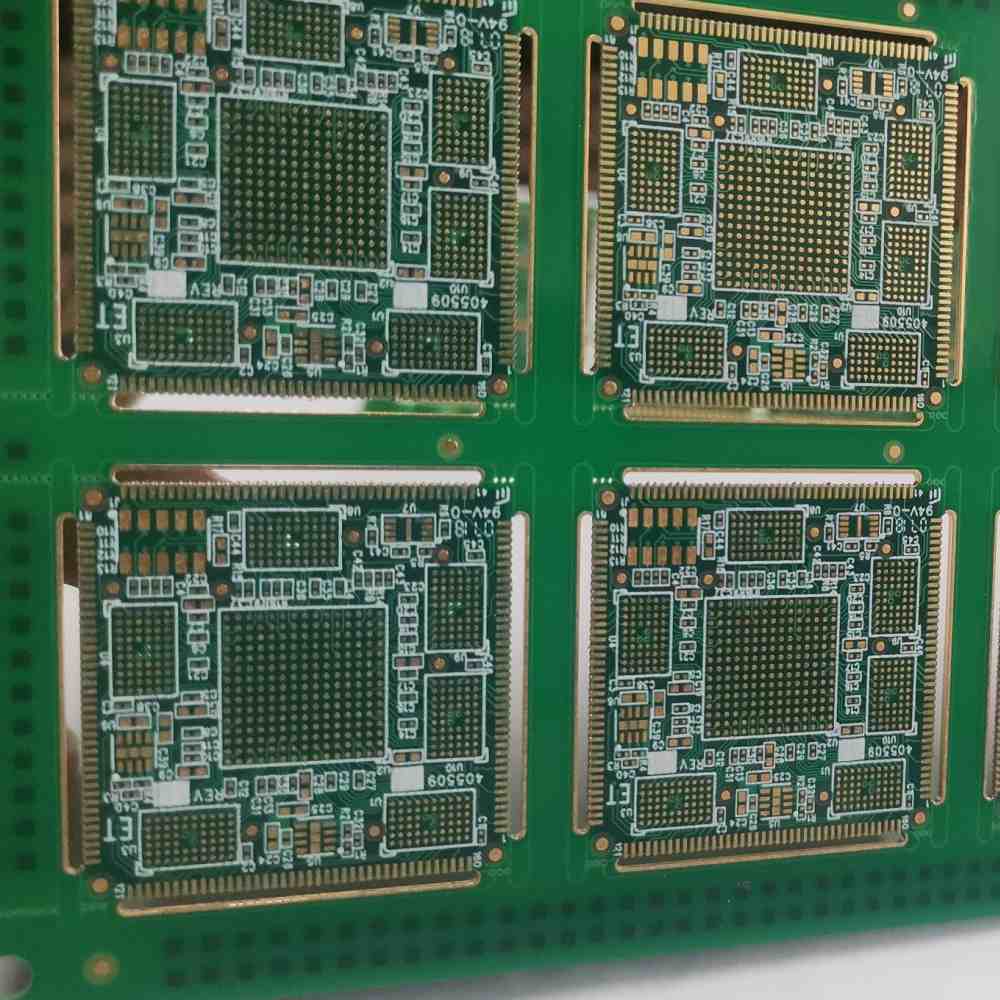
Anylayer PCB Design and Fabrication
Designing anylayer PCBs requires specialized layout tools. Cadence Allegro and Mentor Xpedition offer anylayer design capabilities. The latest versions of Altium Designer and OrCAD also include anylayer features.
The fabrication process is more complex compared to standard multilayer PCBs. It starts with an inner core laminate which is thinner than regular cores. Sequential buildup layers are added to the core with very thin dielectric materials. Microvias are used selectively to connect layers. Blind and buried vias help isolate different sections of the routing.
Special care is needed with stackups, impedance control, and fabrication tolerances. Warpage and thickness variations can affect yields. So anylayer PCB fabrication requires partnerships with specialist vendors having advanced process capabilities.
Conclusion
Anylayer PCB technology opens up the entire board volume for routing flexibility. This enables highly compact and optimized layouts with excellent electrical performance. As electronics become more complex and demanding, anylayer capabilities provide the best solution for routing, miniaturization, and reliability. With sound design practices, anylayer PCBs deliver the density, speed, and precision needed by cutting-edge electronic products.
Frequently Asked Questions
What are the key benefits of anylayer PCBs?
The main benefits are higher routing density, better electrical performance, design flexibility, and miniaturization. Anylayer PCBs allow utilizing the full board thickness for vertical routing. This provides greater density in a smaller form factor.
How many layers can anylayer PCBs support?
There is no specific limit. Current anylayer boards have around 16-24 layers. However, the technology can support 50 layers or more. The layer count depends on design complexity, fabrication capabilities, and budget.
Are anylayer PCBs more expensive?
Not necessarily. Anylayer PCBs require advanced fabrication processes. But they eliminate the need for very high layer count boards to achieve densities. By replacing a 24 layer PCB with a 16 layer anylayer, costs can be reduced.
What are the design considerations for anylayer PCBs?
Careful stackup planning, controlling impedance across layers, managing heat dissipation, and working with tight fabrication tolerances are key considerations. Using anylayer design tools and an experienced PCB vendor are recommended.
What applications are anylayer PCBs suitable for?
They work best for products requiring small size but high complexity like consumer gadgets, defense systems, aerospace avionics, automotive electronics, IoT devices, and medical devices. Anylayer PCBs are also used in high speed computing applications.


Leave a Reply