Introduction
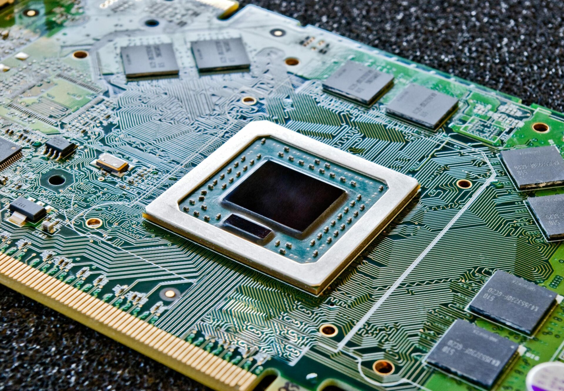
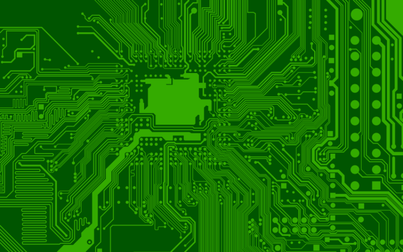
High-density interconnect (HDI) PCBs have transformed the world of electronics by enabling much higher component densities and circuit complexity than previously possible. Traditional HDI PCBs use microvias to interconnect layers and allow traces and spaces under 6 mils. However, these PCBs typically have a limitation: the microvias can only connect adjacent layers due to drilling challenges.
This article explores the emerging technology of any layer HDI PCBs. These revolutionary boards use advanced laser drilling techniques to enable microvias to connect any two layers, not just adjacent ones. This provides design flexibility and optimization not possible with traditional HDI PCBs. We will cover the benefits, technology, design considerations, and applications of any layer HDI boards.
What are Any Layer HDI PCBs?
Any layer HDI is an advanced type of HDI PCB that enables microvias to interconnect between non-adjacent layers in the board stackup. This provides complete vertical interconnectivity, allowing designers to route signals optimally between layers without being restricted to adjacent layers.
The key enabler is the use of laser drilling to create the microvias. Laser drilling can create extremely small “via stubs” that connect layers. The stubs are connected using conventional plated through hole (PTH) vias. This combination enables connections between any two layers.
By contrast, traditional HDI PCBs rely on mechanical drilling of microvias. This process can only drill holes straight down through adjacent layers due to tooling limitations. Any layer HDI breaks through this restriction via laser stubs + PTH technology.
Benefits of Any Layer HDI PCBs
Optimized Routing and Layer Usage
The primary benefit is the ability to route signals directly between non-adjacent layers. This enables optimal trace routing without lengthy workarounds on adjacent layers. Any layer HDI allows the PCB stackup to be utilized efficiently.
Signals can take the most direct interconnect route between components, rather than being constrained by layer adjacency. This is especially beneficial for complex, high-pin count ICs like FPGAs, GPUs, and multicore CPUs.
Reduced Layer Count
By using layers more efficiently, any layer HDI technology can enable PCB designs with fewer layers. The ability to route signals between non-adjacent layers reduces or eliminates the need for transition layers. This can reduce overall layer count by 20% or more versus traditional HDI designs.
The lower layer count results in reduced PCB fabrication costs and may improve yield. It also enables thinner and lighter end products.
Increased Routing Channels
Any layer microvias help relieve routing congestion and maximize routing channels available between layers. With direct any layer connections, signals have alternative paths to use rather than being squeezed into overcrowded channels on adjacent layers. This greatly reduces the complexity of high-density routing.
RF/High-Speed Design Optimization
For RF and other high-speed circuits, any layer HDI enables precise control over critical signals. Traces can be routed on specific layers to optimize impedance matching, signal integrity, crosstalk avoidance, and other parameters. Signals can reference ground planes above or below. This level of control is not possible with traditional HDI.
Flexible Layer Stacks and Blind/Buried Vias
Any layer HDI technology enables numerous layer stackup configurations. Designers have the flexibility to assign layer types (signal, plane, power, etc.) based on optimal circuit needs rather than layer adjacency rules.
Blind and buried vias are also easier to implement, further increasing routing flexibility. Different board areas can use buried vias between inner layers, offering relief for outer layer routing congestion.
Technical Aspects of Any Layer HDI

Constructing any layer HDI PCBs requires specialized materials, processes, and design expertise. Here are some of the technical considerations:
Laser Drilling
As mentioned earlier, laser drilling is the key process enabling any layer microvias. The latest laser tools can drill extremely small “via stubs” down to 25-50 microns in diameter. The stubs connect two layers, often with a larger conventional PTH via in between.
Various laser drilling techniques are used:
- CO2 laser ablation creates via stubs through pulses of infrared laser light. It is suitable for organic substrates.
- UV laser ablation uses an ultraviolet laser focused tightly on the substrate. It has very fine resolution for drilling.
- Picosecond and femtosecond lasers offer high precision with minimal collateral damage.
Via Filling and Plating
The small microvias must be properly plated and filled to create a reliable interconnect. Electroless copper is often used to plate the laser-drilled stubs.
The vias are typically filled with a specialized polymer via fill material using vacuum lamination or injection molding techniques. This prevents voids and allows layers to be stacked up reliably.
Dielectric Materials
Any layer HDI designs require advanced dielectric materials optimized for laser drilling, high frequency performance, and reliability under thermal cycling stress. These include high Tg epoxy, polyimides, PTFE composites, and others. The materials provide a quality foundation for complex HDI board designs.
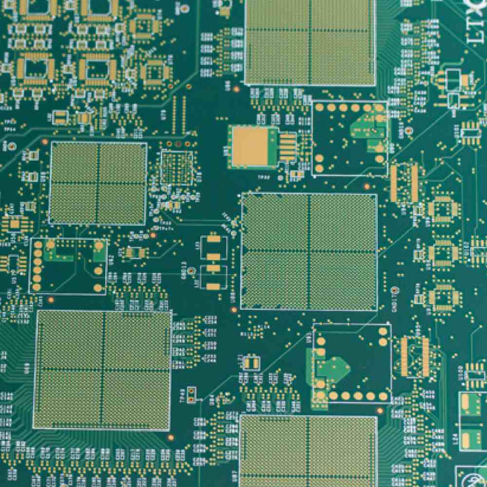
Stackup Design
A key step is planning the layer stackup arrangement around any layer microvias. This defines which layers will interconnect based on signal routing needs. The stackup also balances plane layers for power integrity and impedance control.
Any layer HDI enables greater freedom, but the stackup still requires careful engineering to ensure good performance. This is where experienced PCB designers add value.
Design Considerations for Any Layer HDI
While any layer HDI offers powerful benefits, designers must be aware of some constraints and guidelines when implementing the technology:
Routing Complexity
The unlimited interlayer connectivity poses challenges for routing and documentation. With complex layer transitions, it becomes harder to visualize and verify routing connections. Careful schematic-board correlation is needed.
Microvia Reliability
Although improving, microvia reliabilities are not yet equal to standard PTH vias. Designers should consider factors like via neckdown, capture pads, thermal stress resistance, and stub length.
Minimum Microvia Sizes
The available microvia size depends on contractor capabilities. Laser drilling can produce stubs down to 25 microns, but 50-75 microns is more typical. The layer count also impacts minimum via sizes.
Panel Utilization
Any layer HDI processes often have lower panel utilization since laser drilling is done on individual coupons. Designs should maximize useable PCB area to improve panel efficiency.
Thermal Management
More complex power distribution and filtering may be needed with multiple plane layers. Thermal analyses should be performed to ensure any layer HDI designs can dissipate heat properly.
EDA Tool Support
While improving, some PCB layout tools still have limitations for any layer stackups. Work closely with your EDA vendor to implement any layer designs smoothly. Advanced DRC/DFM tools are recommended.
Applications of Any Layer HDI PCB Technology
Some of the key applications taking advantage of any layer HDI PCB technology include:
High Pin Count ICs
Processors, FPGAs, GPUs and other complex ICs with over 1000 pins are ideal for any layer HDI. The non-adjacent layer routing enables short traces between dense package balls or lands.
Mobile and Wearable Electronics
Thinner, lighter and more integrated mobile devices are driving demand for any layer HDI. The optimized layer count and routing density are ideal for packaged solutions.
RF and Microwave PCBs
Precision routing of matched length traces, controlled impedances, and RF signals benefit greatly from any layer routing flexibility. HDI is prevalent in radio, radar and telecom.
High Speed Digital Circuits
Direct layer transitions without stubs reduce discontinuities in transmission line circuits. Non-adjacent referencing helps control impedances. Any layer HDI is perfect for SERDES, memory interfaces, etc.
Automotive Electronics
HDI PCBs are widely used in vehicle electronics for engine controls, infotainment, RADAR systems, camera modules and more. Any layer HDI enables more integration and reliability.
Medical Electronics
High reliability, small sizes and improved performance enabled by any layer HDI suits medical devices. The optimized routing helps minimize external components too.
Future Outlook
Any layer HDI PCB technology is projected to be one of the fastest growing PCB segments over the next 5-10 years. As designs continue getting more complex and high-speed, any layer HDI provides the interconnection capabilities needed.
Laser drilling technology will continue advancing to enable smaller microvias and more routing layers. Dielectric materials and reliability will also improve.
EDA tools for any layer designs are evolving to make the optimized layer stackups easier to implement. As the technology matures, any layer HDI costs will decrease making it accessible to more applications.
In summary, any layer HDI PCBs represent an exciting platform for next generation, high-performance electronic designs across a wide range of markets. The ability to optimize routing between any PCB layers rather than just adjacent ones revolutionizes HDI capabilities.
FAQ
What are the key benefits of any layer HDI PCB technology?
The main benefits are optimized routing with fewer layers, increased routing channels, design flexibility, RF/high-speed performance, and the ability to use layers more efficiently. Together this enables far greater circuit densities and complexities.
How are the microvias created in any layer HDI PCBs?
Laser drilling techniques such as CO2, UV, and ultrafast laser ablation are used to create extremely small “via stubs” between layers. These stubs are connected with standard plated through hole (PTH) vias.
What size microvias can be produced with any layer HDI?
The latest laser drilling tools can achieve microvia stubs down to around 25-50 microns in diameter. Typical production capabilities are in the 50 to 75 micron range. The via size depends on the laser technique and board materials used.
Does any layer HDI improve reliability compared to traditional HDI?
Overall reliability is somewhat lower compared to standard PTH vias, but constantly improving. Factors like via neckdown, capture pads, and thermal management must be considered, but high lifetimes are achievable with proper design.
What types of components benefit most from any layer HDI PCBs?
High pin count ICs with over 1000 terminals, such as FPGAs, GPUs, advanced processors and RF/analog ICs benefit most from the routing flexibility. Mobile packages are also ideal applications.
Are there any design software tools tailored for any layer HDI PCBs?
Major EDA software platforms like Cadence Allegro, Mentor Xpedition, and Altium Designer have extensive support for any layer stackups, routing, and documentation. DFM analysis tools help validate manufacturability.


Leave a Reply