Introduction
Blind vias are an essential feature in printed circuit board (PCB) design that allow connections between different layers without going all the way through the entire board. A blind via connects an outer layer of a PCB to one or more inner layers but does not penetrate through the entire PCB. This provides several advantages including allowing higher routing density, reducing manufacturing costs, and improving signal integrity for high-speed designs.
In this comprehensive guide, we will cover everything you need to know about creating and working with blind vias in Altium Designer.
What are Blind Vias?
A blind via connects two or more layers of a multi-layer PCB without connecting all the way through the entire board. This contrasts with a through-hole via which penetrates from the top layer all the way to the bottom layer of the PCB.
Blind vias are classified based on which layers they connect:
- Buried Via – Connects two or more inner layers but does not connect to any outer layers.
- Micro Via – Small blind via with a diameter less than 0.15mm or 0.006 inches. Often used in high density designs.
- Staggered Via – A blind via that connects layers on opposite sides of the board rather than adjacent layers.
Advantages of Using Blind Vias
Here are some of the benefits that blind vias provide:
- Increased routing density since traces can route over blind vias on other layers.
- Lower manufacturing cost compared to through hole vias which require drilling through the entire PCB.
- Improved signal integrity at high frequencies by allowing return paths on adjacent layers.
- Enable connections between non-adjacent layers.
- Allow splitting power and ground planes while maintaining connections between them.
Disadvantages of Blind Vias
There are also some potential disadvantages to consider:
- More complex PCB fabrication process requiring depth control when drilling blind vias.
- Increased testing requirements to ensure blind vias are properly connected.
- Not suitable for components leads which need to penetrate fully through the PCB.
- Limitations on the aspect ratio of vias due to drill bit access.
Creating Blind Vias in Altium

Altium Designer provides extensive support for working with blind and buried vias in your PCB designs. Here are the steps to create a blind via in Altium:
1. Switch to 2D Layer Stack Mode
The first step is to define the layer stack for your PCB in 2D layer stack mode. This can be accessed through Design > Layer Stack Manager.
The layer stack defines the order, names, and properties of the layers in your PCB. Make sure to include all layers that you need to connect with blind vias.
2. Draw Blind Vias
Once your layer stack is defined, you can switch back to 2D Layout Mode and start placing blind vias.
To place a blind via that connects from the top layer through an inner layer:
- Switch to the Top Layer view.
- Select the Via tool.
- In the Properties panel, select Blind Via and choose the destination layer.
- Click to place the blind via.
You can view the different connectivity in 2D and 3D modes to confirm the via goes through the desired layers.
3. Define Via Types
It is recommended to create Via Types with your desired via size and hole/annular ring settings. This allows placing vias consistently with the proper settings.
To create a Via Type:
- Open the Object Settings dialog (Tools > Object Settings).
- Select Via Types in the options tree.
- Click the Add button to create a new Via Type.
- Name the new via and define desired parameters including hole size, ring thickness, etc.
4. Set Via Net Tie Rules
You should also set up Net Tie rules to define the connectivity behavior of vias. This determines which net(s) the via will connect when placed in the PCB editor.
To configure Net Tie rules:
- Open the PCB Rules and Constraints Editor (Design > Rules).
- Select Net Tie Rules in the options tree.
- Click Add to create a new rule.
- Set the scope for the rule, such as applies to Blind Vias.
- Define the required Net Tie actions.
Now when you place a blind via matching the rule scope, it will follow the defined connectivity behavior.
Working with Blind Vias
Here are some tips for working with blind vias efficiently in your PCB design:
- Name blind vias appropriately (e.g. BV1, BV2) for easy identification.
- Use offline DRC to catch any improperly connected blind vias.
- Consider limitations on aspect ratio based on your board thickness.
- Minimize use of blind vias with high layer counts due to fabrication complexity.
- Ensure your component footprints support blind/buried vias if required.
- Verify blind via breakout routing meets fabricators requirements.
Modifying Blind Vias
You can easily modify existing blind vias using the following steps:
- Double click the blind via to open the properties.
- On the Structure tab, click the button next to Hole Size to open layer selection.
- Check/uncheck layers as needed to change via connectivity.
You can also change properties like size, hole diameter, and net tie rules.
Creating Buried Vias
Buried vias connecting only inner layers without connecting to outer layers are created similar to blind vias.
When placing the via, simply set the destination layer as another inner layer rather than an outer layer. Use the layer stack preview to confirm the desired connectivity.
Blind and Buried Vias Design Rules
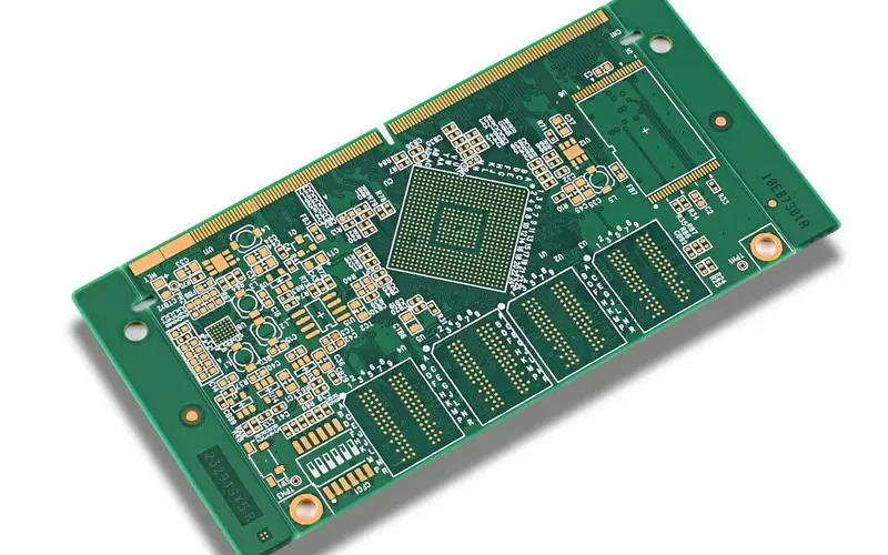
It is important to validate your blind and buried vias usage meets manufacturing design rules. Here are some key guidelines:
Minimum Annular Ring
Sufficient annular ring (copper pad) must surround any drilled via holes to avoid cracking or separation. Common requirements are:
- Minimum 0.15mm annular ring for microvias.
- Minimum 0.2mm for buried and blind vias.
Minimum Spacing
Adjacent vias require adequate spacing to prevent copper overlap or shorts. Typical spacing rules are:
| Via Type | Minimum Spacing |
|---|---|
| Microvia | 0.1mm |
| Blind/Buried Via | 0.2mm |
Aspect Ratio
The via barrel depth to diameter ratio impacts drill bit access and plating quality. Maximum aspect ratios may be:
| Layer Count | Aspect Ratio |
|---|---|
| 6-8 Layers | 1:1 |
| 10-12 Layers | 3:1 |
| 14+ Layers | 5:1 |
Consult your board fabricator for their specific requirements.
Blind and Buried Vias in Altium – FAQ
Q: What is the easiest way to create a blind via in Altium?
A: The fastest way is to select the Via tool, choose Blind Via in the Properties panel, select the destination layer, then click to place the via. Pre-defined Via Types with desired parameters can also be used.
Q: How do I check blind via connectivity in Altium?
A: Switch between 2D and 3D modes to visually inspect via connectivity between layers. The Offline Design Rule Check can also validate connectivity by probing for violations.
Q: Can I convert a through-hole via to a blind/buried via?
A: Yes, you can edit the properties of an existing via to change it from a through-hole to a blind/buried via by updating the layer span in the Via Properties dialog.
Q: What are the main differences between a microvia, buried via, and blind via?
A: A microvia has a small drill diameter (< 0.15mm), buried vias only connect inner layers, while blind vias connect an outer layer to one or more inner layers.
Q: How can I tell if a footprint component supports blind/buried vias?
A: Check the component symbol pins for a Via column – the presence of this column indicates blind/buried vias can be placed. The footprint pads should also have appropriate annular rings.
Conclusion
Blind and buried vias enable advanced PCB design techniques and are a key tool for high density multilayer boards. Altium provides robust support through layer stack management, configurable vias, and design rule validation. Understanding the different types of blind vias along with design guidelines will allow you to effectively leverage them in your next project. Proper use of blind and buried vias provides benefits like reduced drilling costs and improved signal routing while avoiding potential pitfalls.

Leave a Reply